Tekmos Talks Newsletters
A newsletter for the semiconductor industry
Tekmos Talks 2019
|
|
|||
| A Newsletter for the Semiconductor Industry | |||
| December 2019 | |||
| Welcome to Tekmos Talks.This month Product Engineer, Zach Kolb, talks about military testing and we share Inside Tekmos' Thanksgiving gathering. | |||
| From the Desk of the President, Lynn Reed | |||
|
|
|||
| Tekmos Quality Control | |||
|
Tekmos Begins Military Level Reliability by Zachary Kolb, Product Engineer
There are several types of testings we have begun that follow the Department of Defense Test Method Standards for Microcircuits (MIL-STD-883). Some of these methods are not done in house and are sent off to our local reliability counterpart, Criteria Labs who are do tests such as UHAST, Vibration Frequency, and temperature cycle tests. One of the test methods from the MIL-STD-883 we have now begun to use is placing all production parts under a seal/leak test. Once completed and retuned we re-test these parts on sight for a final inspection before they are sent out the door. One of the central tests we use in house to measure product reliability is a Tri-temperature parametric testing. When our microcircuit has been released as a production part our AC and DC parameter tests are also released. In turn, we take our device and place it on our DUT board and then put them under temperature using a temptronic thermostream. We then cool the device under test to -55 degrees C and allow our AC and DC parameters/patterns to run through the part. Once tested we can then see the effects that the lower temperature has on the timing of our devices. With the same thermostream we can test the same device at 125 degrees Celsius. We then compare both temperatures to our room temperature, 25 degrees’ Celsius test. At that point, we are able to identify how various temperatures effect our parametric tests and justify the amount of stress we can have on our products while they are still capable of passing within an acceptable parametric limit. Testing these functional tests at multiple temperatures allows us to conform to MIL-STD-883 for Tri-temp testing. With these tests, we can create our very first FAI reports. The First Article Inspection Reports (FAI) are a new way for us to give our devices a military level reliability and then forward this information on to our clients. As we continue to use these new Test Methods for our part and package reliability it has been noted favorable that even after these different types of stress inducing tests our products remain in-tact and our parts still pass functional patterns.
|
|||
| Inside Tekmos | |||
|
Tekmos Thanksgiving
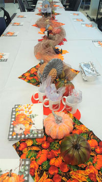
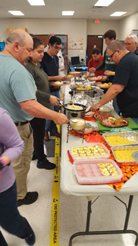
This year, like every year, each team member is asked to bring a favorite food they like to prepare and or want to share with the meal. Lynn prepared his famous deviled eggs, Jon, VP of Operations prepared his grandmother’s apple pie, Alan baked corn bread, Phil got up at 4 am to cook the turkey, dressing, and gravy. Other tasty foods were mashed potatoes, macaroni and cheese, cranberry sauce, corn casserole, spanakopita, a shredded broccoli and cranberry salad, olives wrapped in salami and decorations provided by Alison, our Production Manager. Lynn spoke at the end of the meal thanking everyone for their shared specialties and hard work at Tekmos. Thank you to all our customers around the globe for trusting us with your business.
|
|||
| Thank You for Reading Tekmos Talks | |||
|
Thank you for reading Tekmos Talks and helping us celebrate 20 plus years. Sincerely, Lynn Reed, President
|
|||
|
|
||
| A Newsletter for the Semiconductor Industry | ||
| November 2019 | ||
| Welcome to Tekmos Talks.This month Lynn talks about NRE's, Tyler talks about Inventory Control, and we introduce Inside Tekmos Customer Support. | ||
| From the Desk of the President, Lynn Reed | ||
|
Explaining NRE's To make an ASIC, you have to pay a non-recurring engineering cost (NRE). We’re going to talk about what makes up an NRE. Masks and Wafers A significant portion of the NRE is made up of the mask and wafer charges. This portion of the NRE can vary from a low of $30K to a high of $150K at 110 nm, and much higher for smaller dimension technologies. There are a number of variables in the mask and wafer costs. The first is the technology used. The smaller the dimension, the more expensive the masks. A second variable is the mask type. Using MLM (Multi-Layer Masks) results in putting 3 or 4 different mask layers on a single mask. This can result in up to a 75% savings in mask costs, but it also doubles the wafer costs. As a rough rule of thumb, MLM masks are cost effective when the total production volume will require less than 50 wafers. Tekmos uses gate arrays in many of our designs. If there is a pre-existing gate array that we can re-use for a new ASIC, then we only have to make 6 to 8 masks, instead of the 16 to 27 layers required for a new mask set. And if we can use MLM masks, we can make a gate array mask set using only 2 physical masks. IP Many designs contain external IP that have to be licensed and purchased. While some IP is available for free, most have a cost ranging from $5K to $200K. The IP can range from oscillators to internal memory to external memory and bus interfaces. Also, most fabs charge extra for both the flash IP and the extra masks necessary to implement the flash. Speaking of flash, and depending on the production volume, it may be more economical to include flash die in the package using stacked die assembly techniques than to license the flash IP. We use this approach on our legacy processors for program storage which replaces the old and unavailable EPROM technology. Test Hardware ASICs have to be tested, and we need test hardware to do so. For many digital parts, this can be as simple as soldering jumpers on a device personalization card. Some packages also require the design and implementation of a socketed load board. And analog parts may require the design of specialized measurement circuitry on a custom load board. Some circuits may also require the construction of a probe card. Probing is required when we are selling die, when the cost of the package is high (as in ceramic), or when the design requires testing of pins that are not included in the final package (such as fuse based trimming for analog designs). Engineering Time The last factor of the NRE is the amount of engineering time that Tekmos has to provide. Some designs are ready to go, and only require a minimum of checks on our part. Other designs are in register transfer level (RTL), and must be synthesized and re-simulated. And other designs are “black box” (such as a 27 MHz radio receiver), which require us to do all of the design work. Another engineering task is if we have to write simulations for the design. We come up with an estimate of the engineering time involved, and that becomes part of the NRE. Special Screening Some parts, such as military parts, may require special screening. A major component of those costs is the design and fabrication of burn-in boards for use in burn-in and life testing. Tekmos uses outside services for the non-electrical screens, and each screen has its own lot charge. All of these are added to the NRE. The Final NRE Amount Based on the chip, Tekmos determines what is included in the NRE, and includes them to become part of the final, fixed price quote. And that is how we develop the NRE. Call us to get a NRE quote on your next ASIC project.
|
||
| Tekmos Quality Control | ||
|
Inventory Management by Tyler Sandoval, Inventory Control Manager
Inventory management is a large part of what keeps the manufacturing side running smoothly at Tekmos. Due to the high volume at which parts are manufactured and sold, we require inventory to match up precisely with our accounting software. This is so sales may be able to quote correct quantities available for purchase, as well as start new inventory lots when needed. At the start of each month, our inventory room and test floor is cross reviewed against our digital backlog and adjusted according to the physical inventory we have on hand. It is my job as the inventory control manager to track down any inconsistencies we have, and correct them. This can consist of entering any missing travelers into our database, converting untested stock to finished goods stock, and removing any parts deemed as rejects due to production failures or other testing. Often times, our engineers will need various amounts of parts in order to do further testing into the quality and reliability of our microchips, along with other studies. In these instances, we use a logged tracking system to check in/out parts, record where these parts are going, who has them, and whether or not they will be returning to finished goods to be sold. As our stock levels currently hold over 600 different types of microprocessors for various applications, monthly inventory can seem overwhelming at times. Luckily we have implemented small but impactful changes in the systems we use to make this task a bit easier on everyone. We keep track of our chips using the systems previously described, as well as others such as physically marking inventory boxes to clearly show which parts have had significant movement over the past month, and those that have not. Another way we maintain and keep a strong hold of inventory is in visibility, segregation, and separation. This focuses on where the parts are in their journey from production to customer and how they are marked along the way. When inventory first arrives at Tekmos, it is clearly marked as untested product while being kept in a designated untested area. Once testing has begun, parts are assigned a traveler, listed as ‘At Test’ and noted as to which step in the testing procedure they are undergoing. Parts that have failed testing are moved to a segregated area, marked to be scrapped, or moved to an engineering shelf for future analysis as to why they failed. Good parts are then moved into our finished goods room. From there they are stored until an order is placed for the parts. Once our manufacturing team has received an order, parts are logged, removed, and packed to a customer’s specifications. This may include programming, labels or any other requirements needed by the purchaser. Once packed, the order is shipped out to a customer. If an order is being packed ahead of its ship date, the package is placed on our pre-packed shelf with all the shipment plus customer information, to await shipment. We have various categories in which we store and track our parts to maintain a clean and accurate inventory at Tekmos. These are just a few of the methods we utilize to ensure the timely delivery and production of parts at our company, and to keep everything running smoothly.
|
||
| Inside Tekmos | ||
|
Customer Support
Zeta Angelich recently joined the Tekmos Team as the Customer Support Manager. She brings her years of experience working with people in a wide range of the business spectrum. As Customer Support Manager she is responsible for the development, continuous improvement and delivery of customer service, to key service outcomes for Tekmos customers. Her job is to communicate with Tekmos customers receiving purchase orders, creating sales orders, tracking and coordinating shipment information, consulting with engineers, inventory and production as to when products will be ready. As needed, she engages in the strategic development of operational requirements, process and technology. Zeta enjoyed working 18 years in the music industry of Austin as an agent, director/producer; as a writer, photographer and correspondent of numerous publications; as an Adjunct Professor at a local university, and a marketing/public relations consultant for biotech, petroleum and vineyard industries including semiconductors for Tekmos for seven years. She will continue with marketing and PR for Tekmos. Zeta holds a BA in Communications from St. Edward’s University, an MS from the Graduate School of Business St. Edward’s University, and Viticulture Certification from Texas Tech University.
|
||
| Thank You for Reading Tekmos Talks | ||
|
Thank you for reading Tekmos Talks and helping us celebrate 20 plus years. Sincerely, Lynn Reed, President
|
||
|
|
||
| A Newsletter for the Semiconductor Industry | ||
| October 2019 | ||
| Welcome to Tekmos Talks.This month Lynn talks about Reverse Engineering, Netlist, Automating, and Inside Tekmos, wedding bells again. | ||
| From the Desk of the President, Lynn Reed | ||
|
Reverse Engineering- Netlist Extraction
Last month I discussed the process where we can de-process a chip, photographing each layer as we went along. Then the photographs are combined into a single image. Then the transistors and interconnect are extracted. This process produces a spice level netlist at the transistor level. A transistor level netlist is a correct implementation of the circuit, but is not in a useful format. What we need is a Verilog netlist at the gate and flop-flop level, and with embedded analog blocks and digital memories. How we get there is the topic of this article. Digital Standard Cells Most newer circuits are implemented using standard cells. The software package we use has a built-in pattern recognition. We create a library of identified cells, and it uses that library to extract a netlist. This works reasonably well, and while it does produce an occasional error, those are usually easily identified and fixed. Digital Hand Packed Older chips frequently used manually created layouts. In these layouts, the transistor shapes were modified to fit in the available spaces. This results in circuits where no two gates were alike. And that kills the pattern recognition that we used on the standard cells. We also have cases in modern circuits where later revisions have additional circuitry crammed into the layout using hand-packed techniques. And since pattern recognition doesn’t work here, we must use an alternative approach. Extracting Gates That approach is to extract gates directly from the transistor level netlist. This is an iterative process. The first step is to identify cases where P transistors touch N transistors. These are the netlist nodes, with all other nodes being internal to gates. The next step is to extract those transistors who are part of transmission gates. These are identified by finding pairs of P and N transistors who share common diffusions, but have different gates. These are then removed from the list of unidentified transistors. Then we build a gate, where a gate is defined as a collection of transistors that connect a node with either supply. This step produces a netlist containing the basic inverters, NAND, NOR, and complex gates. Extracting Flops and Higher Level Gates While we now have a Verilog netlist, it does not contain flops, latches muxes, exclusive-or, and similar higher level functions. To get these, the netlist must be processed again. But this time, we look for patterns of logic gates. A 2-input NAND gate that only drives a OR-AND-Invert gate can be replaced by an exclusive-or gate. Error Checking Now that we have a netlist, we have to check for errors in it. Most errors are opens that resulted from errors in imaging. These can be located with Verilog netlist checking tools. And once identified, they can be corrected by examining the original database to see what node the open wire should be connected to. We also occasionally see nodes shorted to supplies, though those nodes are easily visible in a graphical analysis and are usually corrected much earlier in the conversion process. The Next Step Once we have a netlist, then the next step is to do logic simulations to ensure that the design will work in our modern libraries, and does not contain any race conditions. And it must be combined with any analog circuitry that may be present. But that is a topic for another article.
|
||
| Tekmos Quality Control | ||
|
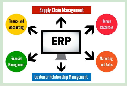
Enterprise Resource Planning Implementation Over the summer we rolled out an Enterprise Resource Planning (ERP) system. The aim of this system is to automate many of the day to day tasks we deal with at a company level and reduce the chance of miscommunication between employees. The system we use is broken down into “Projects” and “Issues”. A Project is what the bigger picture would be, for example, travelers, new engineering test releases, sales orders, etc. An Issue is a single instance of the project, such as a single traveler for a specific part, a new test for a part, or a sales order. Although our ERP system is still a work in progress, we have currently moved our traveler system for testing parts to a digital system and as a result have improved productivity by streamlining the process. To accomplish the traveler system, multiple databases have been created that contain our commonly used setups for hardware, software, and testing. This information is then automatically populated into the travelers. This allows the test engineers to speed up the initial stages by having all the information they need available to them instead of having to ask the engineers for the appropriate setup information. We have also integrated several tablets into the system to allow for the digital traveler to travel (move) with the parts from station to station, in a way similar to how the paper travelers moved with the parts. The databases from the travelers play into the engineering test releases as well. Prior to this system there was never a clear database that was updated with all the approved hardware configurations. When the engineers completed tests, these tests were released to their standards without a universal internal standard. To help with the population of the database another project was created to keep track of these tests. The sales order Project prompts whomever is processing the customer order for the basic information about the order and then sends this information to the next person to work on the order. After the information is entered into the system, an automatic email is generated and sent to the customer informing them that their inquiry has been received and an update with specifics about their order being processed will be sent soon. With this system all of our sales orders are presented in one place with the date they were received and entered, as well as reminders being sent to key people to follow up on the progress of these orders if they aren’t handled in a timely manner. There are still more tasks being automated and moved to the ERP system daily, but, overall, we have had a good start. As time goes on more and more of our daily life at Tekmos will take on a streamlined and automatic approach, making a massive quality of life improvement.
|
||
| Inside Tekmos | ||
|
Wedding Bells
About 75 guests of the families attended including, webmaster Dad, David Abel, Lynn and Carole Reed, Jon Gehm and family, along with numerous Tekmos colleagues. The reception buffet followed at the Chandler in Gruene. Clay and Hannah spent their honeymoon in the Dominican Republic. They will reside in Austin, Texas.
|
||
| Thank You for Reading Tekmos Talks | ||
|
Thank you for reading Tekmos Talks and helping us celebrate 20 plus years. Sincerely, Lynn Reed, President
|
||
|
|
||
| A Newsletter for the Semiconductor Industry | ||
| September 2019 | ||
| Welcome to Tekmos Talks.This month Lynn talks about Deprocessing a Die, Consumer Electronics, and Inside Tekmos, there are wedding bells. | ||
| From the Desk of the President, Lynn Reed | ||
|
Deprocessing a Die As part of the netlist extraction process, we take an original die, and cut it apart one layer at a time. Each layer of the die is imaged with a scanning electron microscope. Then the image in converted into a GDS data base. Subsequent steps extract the netlist from the GDS database. This article shows the deprocessing steps, and the resulting GDS database for a small section of a chip. This particular chip uses a double metal, double poly technology. The section shown is a digital section, and did not use poly2, so that step is skipped.
The 2nd image shows the metal 1 layer. The contacts show up in this layer, but the vias do not. Some of the contacts show up as bright dots, and some show up as dark dots. Fortunately, the software is able to identify both types as contacts. There is a visible shadow on the image left over from etching away the metal two layer. This shadow is ignored by the software. The 3rd image shows the poly1 layer. The diffusion layers also show up in this image. This is a difficult extraction, but can be made easier by looking at the diffusion layer apart from the poly1 layer. The imaging of the poly1 layer can be particularly difficult where it crosses diffusion in the creation of a transistor. There are spots that may have to be manually cleaned up. Removing the poly1 layer makes the diffusion layers show up reasonably well. And speaking of wells, note that the p-well in this process does not show up at all. The presence of a p-well in the digital area can be easily inferred. It is tougher in cases where there may be a p-well resistor in the analog circuitry. [Picture 4- “Diffusion”] This image shows the combined extracted database, which is a portion of a standard cell d-flop. [Picture 5-GDS Layout”] This final picture shows how the software has identified the transistor locations in the layout. [Final Picture “Identify Transistors”] The extraction of the GDS layout is relatively straight forward. Producing the hierarchical netlist from a listing of transistors is more difficult. I will discuss that process in a future article.
|
||
| Inside Tekmos | ||
|
Wedding Bells Kelsey Melhorn, Director of Quality married Cy Casto, in Ocho Rios, Jamaica on August 10th, 2019. About 40 guests of the families attended including, Lynn and Carole Reed, and Jon Gehm and family. The reception buffet was “Caribbean Spice” which included the infamous Jamaican Jerk Chicken! The slang in Jamaica is to say “Yah mon” in every sentence. Jamaican’s live on ‘Island Time’ but are still very organized! It was a stress-free wedding. Kelsey and Cy also spent their honeymoon there where they got to do activities like; scuba diving, horseback riding, kayaking, snorkeling, hiked a waterfall, and lounging around.
|
||
| Consumer Electronic Trends | ||
|
Consumer Electronic Trends in Intelligence of Things
The Internet of Things is passé and no longer the buzzword of the day. Instead, Intelligence of Things (IoT) has moved in as the catchword in the ever-evolving world of technology, with new, faster, and improved consumer technology. The Intelligence of Things achieve more efficient IoT operations, improve human-machine interactions and enhance machine learning, connectivity, data sharing, and analytics. Here at Tekmos we strive to meet consumer electronic predictions. The Consumer Technology Association’s recent research shows consumers want “the benefits of data, sensors, AI and other advanced technologies in the products they own.” The U.S. consumer technology industry is expected to reach a record-breaking $398 billion in retail revenues ($301 billion wholesale) in 2019. Trends are showing that smart speakers have seen the highest jump in the already 95% of US households owning smart TVs, and the 91% of households owning smart phones. The increase in the purchase of wireless headphones, smart/fitness watches and trackers, smart home technology such as thermostats and front door cameras add to the increase in consumer numbers. Consumers expectations are increasing as fast as the technology being developed. People are more open to using smart technologies; using them in their automobiles, to monitor their homes, health, children, and pets. Experts believe the wearable market will reach $25 billion this year. New innovations increase the demand for emerging technologies and consumers are ready to purchase. The Intelligence of Things offers unlimited possibilities, and Tekmos works daily to offer simple solutions to those ongoing complex challenges, designing consumer electronics for your Lifestyle.
|
||
| Thank You for Reading Tekmos Talks | ||
|
Thank you for reading Tekmos Talks and helping us celebrate 20 plus years. Sincerely, Lynn Reed, President
|
||
|
|
||
| A Newsletter for the Semiconductor Industry | ||
| August 2019 | ||
| Welcome to Tekmos Talks.This month Lynn talks about the new and improved Tekmos' website and the trip to Hi-Ten 2019 at Oxford. | ||
| From the Desk of the President, Lynn Reed | ||
|
Tekmos New Improved Website As Tekmos has grown, we have increased our focus on high volume ASICs, and low cost ASICs. To support this effort, we have redesigned our website over the last few months, and made the switch to our new and improved Tekmos website in July. Before starting the transition from old to new, as a team we studied and dissected the current website; the design, flow, and graphics, looked at competitors, and asked ourselves what can we do to improve the site for visitors? We went to our webmaster, David Abel, to guide us along, pulled in our go-to graphic artist, Randy Reed with REEDESIGN and Tyler Sandoval of Tylerphotodesign to add to the mix of art, design and ideas to our regular Marketing team. We took a serious looked at our products and the market, and made some changes on the flow of the website, adding a new template, new content, and more images of Tekmos products. A major change is the inclusion of market focused content. Previously, the emphasis was on legacy products such as microcontrollers and flash memories. Now, we are providing additional content that is focused on our top six markets: Consumer, Medical, Industrial, Aerospace, Military, and High Temperature. Visiting our new site the fresh graphic art icons for Consumer, Medical, Industrial, Aerospace, Military and High Temperature are all visible and linkable on the Home page. Our “Products” page is more user friendly and accessible. We feel the website is a great improvement, and brings Tekmos forward in the Microprocessor, ASIC, FPGA, High Temperature, Legacy product market.
|
||
| Tekmos Events | ||
|
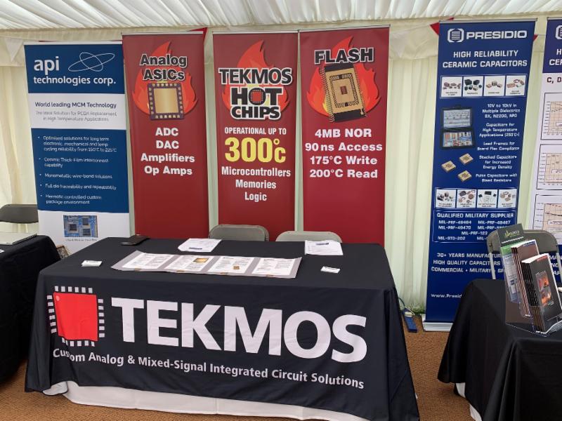
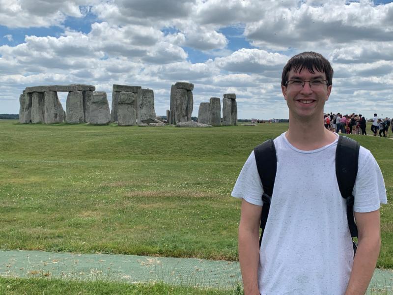
Trip Report: Hi-Ten 2019 Tekmos was a sponsor of the Hi-TEN 2019 conference which was held at Oxford University. Lynn Reed and Clay Abel ran our booth at the exhibit. Exhibit space has always been an issue at Oxford, so this year they erected a large tent for both the meals and exhibits. Fortunately, the weather was unseasonably cool, and so the tent worked out quite well. From a Tekmos business point of view, the conference was a success, with about 150 attendees. We met with multiple prospective customers, and obtained a number of good leads. We also attended some papers, and plan to present at next year’s conference. While Tekmos is seeing nice growth in the high temperature marketplace, we noted that a number of regular exhibitors have dropped out. That was a little unsettling, leaving us with a “last man standing” feeling. As is our practice, we showed up in England a few days early to take advantage of reduced airfares and to allow us to recover from the effects of jet lag. This year, we visited historical sites around Salisbury. This included Stonehenge, the ruins of William the Conqueror’s castle at Old Sarum, the Salisbury Cathedral, and one of the 4 surviving copies of the Magna Carta.
|
||
| Thank You for Reading Tekmos Talks | ||
|
Thank you for reading Tekmos Talks and helping us celebrate 20 plus years. Sincerely, Lynn Reed, President
|
||
|
|
||
| A Newsletter for the Semiconductor Industry | ||
| July 2019 | ||
| Welcome to Tekmos Talks.This month Lynn talks about our new Tape & Reel, we'll introduce Clay Abel, Engineer, and share about our Summer Interns. Tekmos sponsors IMAPS Hi-Ten 2019 Oxford UK 7/8-10/2019 | ||
| From the Desk of the President, Lynn Reed | ||
|
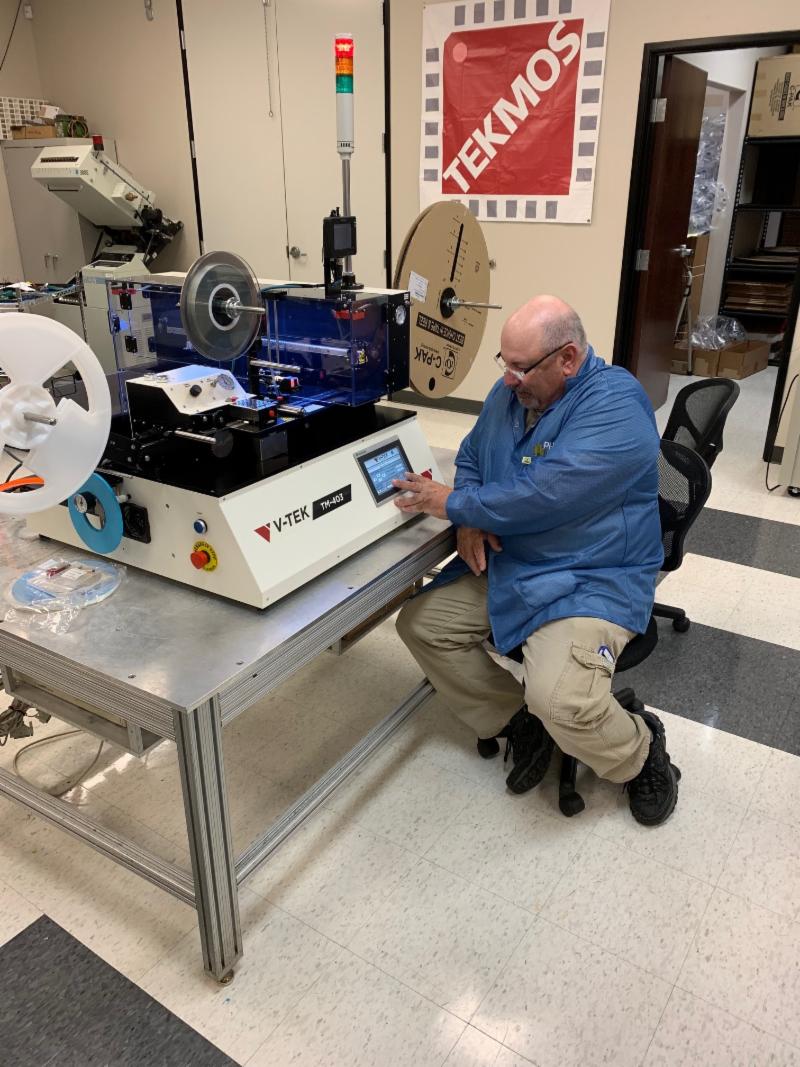
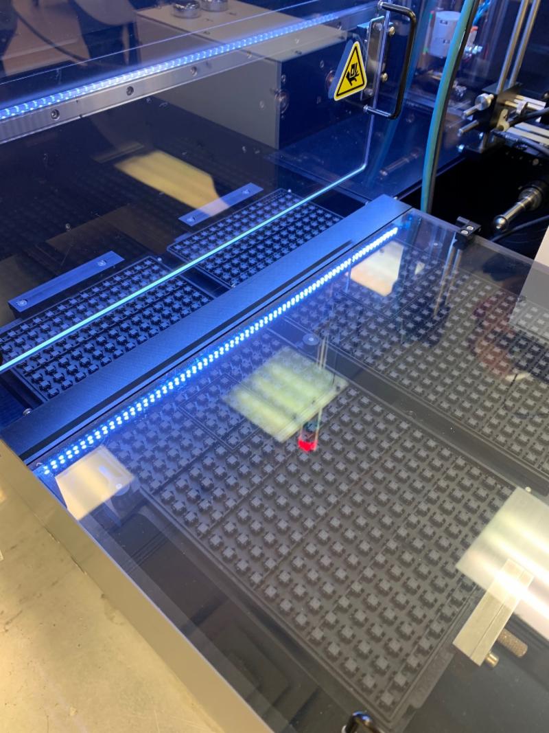
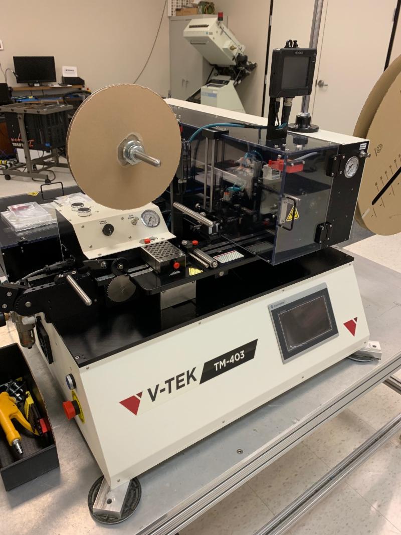
An Increase in Tape and Reel Capacity As a fabless semiconductor company, Tekmos outsources wafer fabrication and device assembly. The decision to outsource testing is more complicated. As a basic philosophy, Tekmos would prefer to do all testing in-house. This is driven by a need to control a major component of the manufacturing and to insure that our customer’s priorities are being met. But we occasionally get either product types or package types which we cannot do in-house, and so we outsource the testing of those parts. The deciding factors are a combination of pin-count and package type. Our largest tester has 320 data channels and can support parts up to about 400 pins. If the pin count is higher than that, we will have to either design a custom tester, or outsource testing. The package type and its associated volume is another factor in deciding to outsource. Any part can be manually tested, but manual testing is slow, and so we only use it for low volume parts. Higher volume parts have a lower cost, and are more sensitive to the test cost. Tekmos has a number of handlers, and tape and reel machines, but we don’t have the capability for tray-fed tape and reel. Or at least we didn’t until last month. In the last year, we have seen a large increase in our consumer products volume. And since most consumer ICs are QFN devices that are sold in a Tape & Reel format, we have needed to increase our T&R capacity. Our current machines are tube fed, but we needed to get one that was tray fed to handle the QFN packages. So, we purchased a second Tape and Reel machine. Our new machine has a capacity of about 2000 units per hour, which translates to about 15K units per day with a single shift of operation. It also has an optical inspection capability, that checks to make sure that the package is orientated correctly in the tape before it is sealed. Now that we have fixed our tape and reel capacity issue, our next capacity problem is in the area of QFN handlers. And I will address that in another article.
|
||
| Meet Tekmos | ||
|
Clayton Abel, Design Engineer I graduated from Abilene Christian University with a Bachelor of Engineering degree. As for what I have been doing since graduation it sure doesn’t feel like it has already been a year since I have graduated. When I first started full time at Tekmos I was mostly shadowing the senior engineers, learning and doing as much as I could to be useful. My first large project was working with John and testing the design of the FIFO part for BAE. I oversaw writing code to stimulate his design and make sure that his design met all the timing requirements in the datasheets. After that I designed and built a burn-in board, using a program called Design Spark, so that we could test multiple of those parts in the oven at one time. My next big task was to design a test for the TK7852E and TK7852L which are both BAE parts. For these parts, we had to program the internal oscillator to a specific value that is different for each part. I needed to figure out a way to test a part and program to the necessary value all at the same time. I wrote some scripts that would look at the test log and calculate the necessary value and then program each part. I have also overseen the testing of these parts and writing the First Article Inspection Report for these parts. One part of the First Article Inspection Report that I have been working on recently was three programs that work together using the test log from production to extract all the necessary data and put it into an Excel file that is formatted to match the Data Sheet. This program will make future FAI Reports a lot easier because you won’t have to sift through large files and manually take out the data you need. I made it as user friendly as possible so that anyone who needs to do one of these reports in the future will be able to easily use my program. I have also been working on a High Temp Flash part, I designed and made a test board with space to attach 10 parts so we could do our initial testing which was used to verify that the part does work at and above our temperature range. I have also designed a single socket board that will be used for production in the future, and my next step will be designing a burn-in board for these parts so we can test multiple parts in an oven all at the same time. I am also tasked with designing a section of one of our new chips that we will be working on soon, so I am looking forward to that.
|
||
| Inside Tekmos | ||
|
Summer Intern Program Each summer, Tekmos hires summer interns. Generally, these are electrical engineering students, though we occasionally include mechanical engineers and computer science majors as well. Many interns started working for us in high school, and have come back each summer while in college. Two of our current engineers started out as interns. We try to increase their responsibilities each summer, matching the increase in their knowledge as they near graduation. This summer we have seven interns. Two are senior electrical engineers. Jacob Rogers is a senior at Texas A&M. He has been working on an interface between our testers and a new multi-site handler we have purchased. The tester uses a parallel interface to control the handler, and the new handler requires a serial interface. The solution is a raspberry pi, an interface card, and some software. Isabel Hegedus is also a senior at Texas A&M. She is working on the DSP algorithms we will use to test a codec in a telephone application. We are trying to deliberately distort a sine wave input in a manner that will cancel out the distortion that is added by digital sampling. This results in a cleaner signal internal to the chip, which makes it easier to use FFT processing to determine idle channel noise and intermodulation distortion. Last summer, Isabel worked on the design of a constant frequency oscillator, which included a voltage regulator, a bandgap voltage reference, and a bias generator that compensated for variations in process, temperature and voltage. Johnny Chen is a senior MIS major at the University of Texas. He is working on electronic travelers which are a part of our internal ERP system. We are linking the travelers into a database that contains test and shipping requirements as well as any special instructions. Carter Gehm is a senior mechanical engineering major at Texas A&M. He is designing and installing a nitrogen purge system for our bake and life-test ovens. The system covers the nitrogen source, pressure regulators, piping, flow meters, and oxygen sensors for safety. Gavin May will be starting college this fall as an engineering major at UC Berkley. Gavin has worked with us during high school doing some programming to allow the automatic collection of oven temperatures. Since he was already programming for us, we have put him working with Johnny on our electronic travelers. Ryan Gehm is another high school graduate who will be starting in electrical engineering at Texas A&M this fall. Ryan is working with another of our engineers doing the first article inspection of a new military product. Chris Hoenig is starting his Junior year in high school. Chris is working on our test floor, feeding handlers and running our tape and reel machine. We consider the summer intern program to be a win-win situation. We benefit by having additional resources work on lower priority problems that might not get done otherwise. And the students gain work experience that will help them stand out from the other students as they begin their job search after graduation. |
||
| Thank You for Reading Tekmos Talks | ||
|
Thank you for reading Tekmos Talks and helping us celebrate 20 plus years. Sincerely, Lynn Reed, President
|
||
|
|
||
| A Newsletter for the Semiconductor Industry | ||
| June 2019 | ||
| Welcome to Tekmos Talks. This month Lynn talks about High Temp Flash, 9 Die in Package, and Tekmos new machines. | ||
| From the Desk of the President, Lynn Reed | ||
High Temperature Flash Memories A challenge in high temperature electronics is the availability of flash memories. To address this, Tekmos is offering up-screened flash memories that are rated at 175C and 200C. More specifically, the first part is the TK29H400AT-70, which is a 4MB, 3 volt, top-boot sector, 70 ns NOR flash memory, This article will discuss the issues in up-screening flash memories to work at elevated temperatures. To up-screen a part, it is necessary to test each parameter to guarantee compliance with the specification. And in the case of high temperature operation, it is also necessary to address reliability issues and technical issues. Functionality The first question to be addressed is if the part is functional at high temperature. Flash memories have a fair amount of analog circuitry which is used in the sense amplifiers, the programming charge pump, voltage references, and the brownout detect. This circuitry was typically designed for functionality over a -55C to 125C range. But will it still work at 175C or 200C? The only way to find out is to run a part at those temperatures. We took some of the 4M flash die we use in our microprocessor parts, and assembled them in ceramic packages. We then wrote a test program for the flash, and verified correct operation at room temperature. Next, we used our temperature forcing probe, and characterized the part at increasingly higher temperatures going up to 200C.
Reliability The main reliability concern in a flash memory is data retention. How long will a flash hold its memory? As a very rough rule of thumb, the data retention time halves for every 10C rise in temperature. The 10 year guarantee at 85C starts to look more like 1 week at 175C, and a few days at 200C. Fortunately, this can be addressed by refreshing the flash. There are strong limits on the number of times a flash can be erased, but the same data can be re-written many times without degrading the parts performance. JEDEC specification JESD22-A117E covers the testing of flash endurance and data retention. We are running these tests now to verify the upscreened part reliability. Testing When up-screening, each part has to be tested at temperature. Unfortunately, there are no commercially available test sockets that will work in the 200C range. As a result, the test socket has to be custom made out of high temperature materials. The socket difficulties were one factor in our choosing a 56 pin package for the high temperature flash parts. That way, we can reuse the same hardware for a number of different sized flash memories. Packaging The plastic used in packages decomposes at elevated temperatures, so the only practical solution is to use ceramic packaging. There are also reliability issues with gold bonding on aluminum pads, so the bonding has to be done either with aluminum wires, or the pads have to be replaced with a nickel-palladium-gold coating. We are choosing to go with aluminum bonding. Future Work While we are currently working with 4MB flash memories, we plan to extend this work up into 64 MB flash after we finish with the 4MB parts. Availability The TK29H400A is priced at $225 in 100 piece volumes, and is available now in limited quantities.
|
||
| Tekmos Unify Program | ||
|
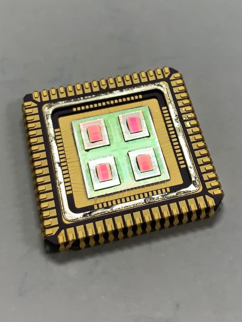
Nine Die in a Package The Tekmos Unify program combines multiple die in a single package. Typically, this is done to save board space in size critical applications such as implantable medical electronics. We recently came across a different requirement where we were replacing an obsolete hybrid module containing 5 volt SRAM and flash memories. Since 5 volt flash memories are no longer available, we created an ASIC that supplied both a 3 volt power supply and had level translators to support the different power supply domains. The final product contained our ASIC, four 512Kx8 SRAMs, and four 512Kx8 flash memories. The ASIC was large, at 12 mm per side. The ASIC size was dictated by the size of the stacked memories. Since the voltage regulator are not that large, we used the rest of the ASIC space to create large decoupling capacitors to assist with the high speed SRAMs. Above is a picture of the final product. There are three different types of die in the package, each from a different wafer fab, and each type has slightly different oxide thicknesses. This causes each die to have a slightly different color. The large green die on the bottom is our ASIC. The white die are the SRAMs, and the red die are the flash memories. Each stack of die is 512K bytes, with the overall chip having 512K of 32-bit words. Having parallel stacks of die led to some interesting bonding problems. Between the stacks we have two sets of staggered pads, for a total of 4 rows. We had to separate the staggered pads so that the back end of the bonding tool would not damage the second set while bonding the first set. The ASIC has 387 bond pads. We needed to probe the device, but did not want to invest in a complicated probe card that could cover 8 vertical rows and 4 horizontal rows of bond pads. So we added a type of scan circuitry that allowed us to verify the connectivity and operation of all the internal bond pads. We also brought out the four voltage regulators so they could be tested. Come talk with us to find out how we can provide a simple solution for your complex problems.
|
||
| Tekmos Upgrades | ||
|
Tekmos Upgrades our Manufacturing Capability with a New Tape & Reel Machine Like many semiconductor manufacturers, Tekmos uses a combination of in-house capability and external subcontractors to manufacture its products. And while we will never have our own fab and plastic assembly, we have a goal to maximize the testing we do in-house. We currently run a tube-fed tape and reel machine in-house for our PLCC and SOP parts. But, we have had to outsource our QFN tape and reel requirements. That outsourcing has now ended with the purchase of a tray-fed tape and reel machine. With a capacity of 2200 units per hour, this machine doubles our current T&R capacity. |
||
| Thank You for Reading Tekmos Talks | ||
|
Thank you for reading Tekmos Talks and helping us celebrate 20 plus years. Sincerely, Lynn Reed, President
|
||
|
|
||
| A Newsletter for the Semiconductor Industry | ||
| May 2019 | ||
| Welcome to Tekmos Talks. This month Lynn talks about low cost methods for including Flash in Designs and a trip report to the Consumer Electronics Show in Vegas, and our Director of Quality shares about Tekmos' BSI AS9100D certification. | ||
| From the Desk of the President, Lynn Reed | ||
Low Cost Methods For Including Flash in Designs Including flash on an ASIC die involves tradeoffs. While flash is available in most processes, you need to be using a process of 90nm to 65 nm to start obtaining reasonable flash densities. But these processes have a substantially higher NRE, which is only justifiable with higher volumes. This is a particularly painful tradeoff when all of the other requirements can be met with a 130nm, 180nm, or even a 350nm technology. Another complication with flash is that each die requires a data retention test, which consists of writing a pattern into the flash, and then baking the wafer for a day at around 250C, followed by a second probe test that verifies that the pattern is still present in the flash. The cost of test is a significant factor in the final product cost, and adding two additional tests is a serious increase in product costs. Flash manufacturers mitigate this cost using special probe cards that can probe an entire wafer at the same time, but this is generally not feasible for an ASIC. Our preferred approach is to purchase flash KGD (Known Good Die), and assemble the part on top of our ASIC in the same package. The flash and the ASIC can be background so that they will both fit in the 0.8mm thickness of a QFN package. The assembly cost does rise by an amount related to the number of additional internal bond wires, but this can be reduced if it is possible to use a serial flash in the application. And either way, the increase in assembly cost is much less that the increase of test costs for embedded flash. There are design challenges with interfacing an external flash with the ASIC requirements. Writing to, or erasing the flash can make it unavailable for code execution. The bus width of the flash may not align up with the chip requirements. And the flash access time can act as an upper limit on an embedded processor’s speed. There are design techniques that can be used to address these challenges. A small ROM can be included that will contain the processor code for flash write and erase operations, though care must be taken to deal with interrupts that might occur during flash operations. The bus width and speed requirements can be met by transferring the Flash contents to RAM for execution. And the use of cache can allow the execution of code out of a large amount of flash. Tekmos has used this technique to add flash to our designs for 18 years. It is used in all of our microprocessors, and in our flash memory offerings. Contact us to find out how we can add flash to your SOC application.
|
||
| From the Desk of Kelsey L. Mehlhorn, Director of Quality | ||
|
Revamping Quality Effectiveness and efficiency are two words usually defined in an organization’s Quality Management System. Companies aim to develop efficient processes and procedures that are effective to the overall goal of the institution. Tekmos’ strategic goals incorporated a focus on designing Application Specific Integrated Circuits (ASIC) to the military and aerospace industries, and our management team decided Tekmos needed more vigorous controls, credibility, and overall Quality System in order to exceed supplier-customer relation expectations for those industries. Which is why Tekmos decided to upgrade our ISO 9001 Quality System to the superseded, AS9100 Rev D Quality System. Although Tekmos had a quality team ready to take on the new AS9100 implementation, we decided to hire a consultant who was experienced in the AS9100 requirements to equip our quality team with the best practices and methods. Working with a consultant gave us a calming relief that we were headed in the right direction. Our consultant was able to find our weaknesses and strengthen us at the core. Tekmos made many adjustments while enforcing the newly acquired quality requirements. These changes challenged us to break old habits, and have employees step up into leadership positions to oversee department performance metrics. With this new leadership team, we have been able to have thorough Management Reviews which establish a clear path of communication between the employees needs and management’s resources. A major advantage Tekmos gained from transitioning to the AS9100 Quality System was being able to integrate the preceded ISO 9001 requirements with new risk prevention and mitigation programs. Potential risks are assessed with 3 key ratings; Impact, Probability, and Resolution. If a risk were to have a high rating, a mitigation program will be enforced to help prevent the risk from occurring. This helps plan future contracts while looking from a risk based perspective which ultimately eliminates unforeseen complications with stakeholders. We are very proud of our employees and the hard work they put into making the transition possible and for continuing to comply with the new quality system as the years have gone by. As Tekmos moves forward with ASIC designing and other customer demands, we will ensure customers that our Quality Management System has been developed to better our customer communication, seek continual improvement, and encourage effective and efficient processes. Although Tekmos has completed the AS9100 qualification that is not stopping us from continuing to implement more industry recognized standards. Tekmos is currently transforming our Information Security System to be compliant with NIST-800-53 standards. This gears us to have a secure Information System for any and all sensitive data we might receive from government projects If you would like a copy of our AS9100 Quality Certification, please visit our website’s support page.
|
||
| Consumer Electronics Show, Las Vegas | ||
|
Bob Abrams and I visited the Consumer Electronics Show in Las Vegas. We go to meet with prospective customers, and to study the market to see which areas are growing and that might need ASICs. The CES show is huge, and the largest show held in Las Vegas. In addition to the Convention Center, it spills over into two other hotel convention centers. The show is subdivided into sectors, such as automotive, gaming, audio-visual, and health. And while we visited all of the sectors, we concentrated on the fitness, health, and lifestyle sectors. Here are my observations. There is a large market in fitness monitors, though the size of the devices is still large. This provides an opportunity for custom circuits to reduce both the size and power requirements for this application. So far, no one has been able to optically measure blood sugar, which remains the holy grail of monitoring. There were a large number of baby and pregnancy monitors. I was impressed with the appearance of small, low cost ultrasound machines. They were being marketed mainly to doctors, but the manufacturers hoped to penetrate the home market as the prices continued to fall. The image processing software for the ultrasound probe also showed improvements in noise reduction and in better imaging the baby. International Harvester showed one of their tractors that worked with GPS to achieve 3-inch location accuracy. This is necessary for it to be able to drive around the fields without crushing the crops. They did it with a combination of GPS and GLONAS receivers, and local transmitters that generated a GPS error connection signal. The machine was huge, perhaps 20 feet tall and 30 feet wide. I found it incredible that it could travel the fields with such an accuracy. The large TVs were impressive, though their 8K resolution exceeds the available programming. The most impressive TV I saw was in the basement of one of the hotel convention centers. A French company demonstrated a 3D TV set that worked without the need for 3D glasses. They had a grooved screen that allowed each eye to see a slightly different image. The automotive section was a little disappointing. While many manufactures presented concept cars, I did not think that any of them exceeded the capabilities of the Tesla that our IT manager drives. I think that you are in trouble when your car of the future is behind a car that is already available. I will wrap up with a few personal notes. We made late reservations, and so we stayed at a bottom of the line casino. We compensated by eating in the nicer places. And we definitely got our exercise. I count steps, and we did more than 25,000 steps each day we were there.
|
||
| Thank You for Reading Tekmos Talks | ||
|
Thank you for reading Tekmos Talks and helping us celebrate 20 plus years. Sincerely, Lynn Reed, President
|
||
|
|
||
| A Newsletter for the Semiconductor Industry | ||
| April 2019 | ||
| Welcome to Tekmos Talks. This month Lynn talks about new ways to reverse engineer a chip, the TK80C51 revision, and we are happy to announce Tekmos' new Customer Service Manager, Shannon White. | ||
| From the Desk of the President, Lynn Reed | ||
New Ways to Reverse Engineering a Chip Tekmos frequently finds itself creating a new chip to replace one that has been discontinued. Traditionally, we studied the data sheet and measured the chip performance on our tester, and then designed a replacement part. This method works, but has one flaw in it. You can only verify what you test. We test everything that we can think of, but if we overlook a situation, then that case might not work. This results in an errata for the part, and possibly a product revision. Microprocessors are more difficult than most chips because they have almost unlimited numbers of initial conditions, and many events are asynchronous. Just adding two 16-bit numbers with carry creates 8 billion combinations, and it is not practical to test them all. Asynchronous interrupts can occur at any time during the execution of any opcode, providing another large set of events of which we can only test a few. To get around simulation limitations, we frequently build FPGA-based emulators for our designs, and run them in customer systems to detect rare combinations. This is a good approach, but is limited by whatever code is running. Over the past several years, a new technology for netlist extraction has developed making it much easier to extract a design from an existing chip. This technology was originally developed to meet the needs of patent attorneys who were examining existing parts looking for patent violations. In this technology, a chip is imaged using a scanning electron microscope (SEM). The top layer is removed, and the chip is re-imaged. The process is repeated until all the chip layers have been individually imaged. Specialty software converts the images into a GDS data base of the chip. Additional software extracts the individual transistors and resistors, and produces a spice netlist. This netlist is further processed to produce a Verilog netlist at the gate level. This netlist becomes the starting point for our work. The first thing that we check for is to make sure that the netlist does not contain opens or shorts. If we find one, we go back to the images to see what is going on. Removing the layers is an art more than a science, and it is possible that the part can be damaged in the process, resulting in errors in the netlist. Next, we have to evaluate the design. We have better design tools today that those that existed when many of these circuits were originally made. We use these tools to find possible race conditions or process sensitivities that may have existed in the original parts. Better tools, combined with improvements in modern process parameter controls, means that we can produce a functionally identical part with superior AC and DC characteristics. For example, many older parts were offered in a 70ºC commercial temperature range and an 85ºC industrial temperature range. Usually, a 70ºC part would stop working at 85ºC, which is not a lot of margin. With a more robust design combined with tighter process controls, we frequently exceed even the military 125ºC temperature specifications. Because of the benefits in producing an exact duplicate, Tekmos has switched over to netlist extraction as the preferred technology for recreating obsolete parts. |
||
| TK80C51 Revision | ||
|
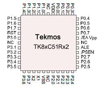
As part of our transferring product to our new fab (X-Fab Dresden), we expanded our 80C51 offering by adding flash-based program storage. This allowed us to offer replacements for the 87C51Rx2 devices. These devices contain 256 bytes of XRAM in addition to the 8K, 16K, 32K, or 64K bytes of program storage. The XRAM is enabled through a bit in the AUXR register. In the 87C51Rx2 series, this bit powers up in a zero state, which enables the internal XRAM to be active in the address space 0000h to 00FFh. This poses a backwards compatibility issue between the ROM-less part 80C51RA2 and previous 8051 variants, such as the 80C51FA, and the older 80C51 and 80C31 parts. Our revision changes disable the internal XRAM for those cases where we are not using the program storage flash. This makes the part backwards compatible with the older 80C51 parts. We also took advantage of the revision to increase the dynamic current on the output ports. It was running on the low side, and we raised it to a nominal value that lies between the average currents of both the NXP and Atmel parts. The previous version of our *xC51Rx2 parts will still be available to customers that do not want to qualify the newer part. To learn more contact: Sales. |
||
| Inside Tekmos | ||
|
Tekmos' Customer Service Manager, Shannon White
What brought you to Tekmos? I actually was brought here through a mutual church group friend of Kelsey and mine who knew that I needed a job and he placed it on a job page with my contact information. Through the grapevine I was contacted about the position and received an interview. What are your responsibilities here at Tekmos and what do you hope to do to improve Tekmos customer service? I have many responsibilities at Tekmos but the main responsibility is making sure the customers are happy and want to continue coming back to Tekmos. I answer the phones, place orders, correspond with clients to make sure they have everything they need, and help with shipping and receiving. I hope to assist in making it easier to help the customers. What are your favorite tasks or projects to work on here at Tekmos? My favorite tasks are correspondence with the customers and clients. I am a people person so this comes naturally to me. I also love learning more about this field as I am working on my BA in Computer Sciences online as we speak. What Project are you working on now? I have so many projects in my daily schedule however, I am assisting in gathering and updating all client information for the company. Tell us about your professional and educational background. I have a degree in Criminology, a Physical Therapy certification, I’m completing my BA in Criminal Science online, I want to get my BA in Physical Therapy next, and have over 20 years of construction and Executive Administrative experience. I’m a "Jane" of many hats. |
||
| Thank You for Reading Tekmos Talks | ||
|
Thank you for reading Tekmos Talks and helping us celebrate 20 plus years. Sincerely, Lynn Reed, President
|
||
Main Office
Tekmos, Inc.
14121 Highway 290 West
Building #15
Austin, TX 78737
Phone: (512) 342-9871








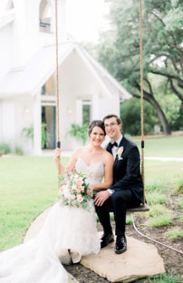 Clayton Abel, Design Engineer, married Hannah Markert in Gruene, Texas on September 1, 2019.
 The first image shows the metal 2 layer. The vias show up well in this image, so we can extract both the metal 2 layer and the via layer. Conductive layers show up brighter in a SEM micrograph. But only the metal 2 layer shows up. The metal 1 layer in under the intermetallic layer, and so does not appear bright in this image. This is good, since if the metal 1 layer was visible, then it would be much harder to extract the metal 2 layer from the image.



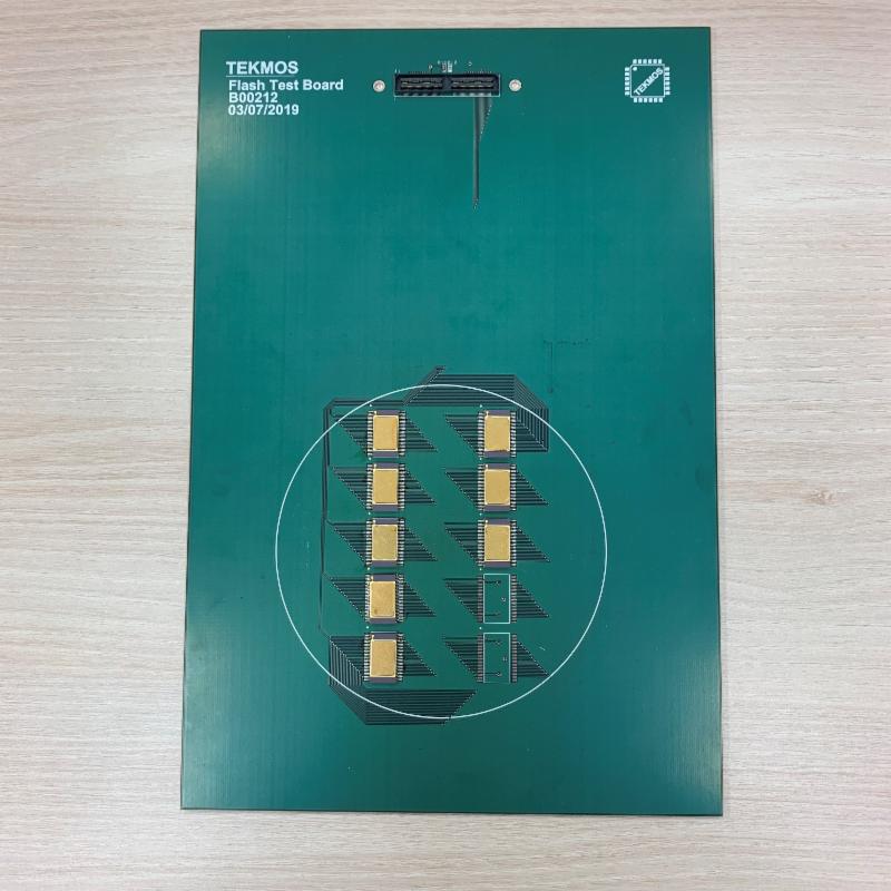 To the left is a picture of the test hardware we used to characterize the flash memories. The area was constrained by the physical size of the temperature forcing probe, which is shown by the circle. And we opted to solder the parts to the board, which temporarily bypasses the problem of high temperature sockets.