Tekmos Talks Newsletters
A newsletter for the semiconductor industry
Tekmos Talks 2016
|
|
||
| A Newsletter for the Semiconductor Industry | ||
| December 2016 | ||
|
Welcome to Tekmos Talks December 2016. This month we will share part II on Block Ram, talk about Tekmos' MCT Handler, and share Inside Tekmos Fall Camp Out. |
||
| From the Desk of the President, Lynn Reed | ||
|
Dual Port RAM Design - The Bit Design Goals It can be asked why design a dual port memory bit? Is this not a case of re-inventing the wheel? Not necessarily. Most memories are designed with speed being the main design goal. You achieve speed by limiting that range of voltages and temperatures that the memory will operate over. In our case, our main goals are reliability and robustness. We serve military, medical, and industrial customers whose applications frequently push the voltage and temperature limits. We do not want the memory to be the weak link in the design. RAM design begins with the bit. It is amazingly complex for a design that has only three types of transistors. The bit consists of a pair of cross coupled inverters, and a pair of N-channel transmission gates that are connected to the bit lines. In the case of a dual port memory, there are two pairs of transmission gates. The first requirement for the bit is that all transistors be as small as possible. This bit is replicated millions of times, so the bit area must be minimized. The second requirement is that the bit must be writable. The transmission gate transistor must be strong enough to pull the inverter output low enough so that the bit toggles. A third requirement is that the bit must be readable. That is that the transmission gate must be weak enough so that the bit line capacitance does not cause the bit to toggle when being read. Or more specifically, approach a meta stable value that would allow noise to easily toggle the bit. A fourth requirement specifically for the dual-port bit is that any operation on one port on a specific bit cannot interfere with the operation of the other port on that same bit. And finally, the bit must work over all combinations of voltage, temperature and process variations. This particular technology uses a 1.8-volt supply. Still, we would like for the memory to work with supplies of 1.5 and 1.2 volts, and over temperature ranges from -65ºC to +150ºC. And we will try to get it to work up to 200ºC. For convenience, we will refer to the inverter transistors as "P" and "N", and the transmission gate N-channel transistor as "T". Writing the Bit The worst case for writing a bit occurs when we are trying to toggle the bit while the other port is reading it. The "T" that is setting the bit must overcome both the "P" pulling up, and the other "T" that is attached to the precharged bit line. For simulation purposes, the bit line can be assumed to be tied to Add. In reality, the bit line is a large capacitor that is precharged to Vdd. Assuming that it is directly connected to Vdd is a worst-case assumption, and if the bit works with that assumption, then there will never be any problems with using the bit design in larger memories. Reading the Bit The danger in reading the bit is that the "T "devices will pull the low node in the memory up to a point where it can switch state in the presence of noise. The worst case occurs when both ports are reading the same memory bit. You have two "T" s pulling up and one "N" pulling down. Also, the stronger the "N" device, the lower the switching threshold, which makes the situation worse. Increasing the strength of the "P" raises the threshold, but makes it harder to write to the memory. There are no free lunches in nature. Running Spice We run spice to determine the optimum sized for the "P", "N", and "T" transistors. There are an almost infinite number of choices in transistor sizes, and there is not enough time to check them all. So, the best approach is to start with a previous solution, and then vary individual transistors until an optimum is reached. Because individual processes and process nodes vary from each other, each process will have its own optimum device size. The layout also introduces limitations on device sizes. To achieve a given W/L ratio, one can vary either the width or the length. Normally, the length is the process minimum, but sometimes it is better to modify the length, and allow the width to be set by layout concerns. The Layout Once the transistor sizes are known, the layout can be competed. The best bit layout was determined a long time ago, so it is a matter of adjusting the sizes and spacings to match your particular process. As an option, you can introduce a little bit of asymmetry into the layout diffusions so that the bit will tend to power up in a known state. This is not required, but is a nice feature. Along with the bit, we also design a dummy bit, whose output is always a zero. This will be used in the self-timing logic. We also have to design a set of substrate contacts that will be inserted every 8th bit. This saves space as contrasted to including them in every bit. Future articles will discuss the word line driver, the sense amps, and the RAM timing controls. |
||
| MCT Handler | ||
|
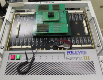
MCT Handler
While old, the handler is capable of both hot and cold operation, and can test parts at a 1800 uph rate. The handler has a clever mechanism that reverses the part orientation during test. Parts that are fed into the handler with pin 1 first, and leave the handler with pin 1 last. This allows a tube of continuity rejects to be easily retested. We also use this handler in our programming operations. We pre-program about half of our micro controllers, and to do so, we use the combination of our production tester and the MCT handler. The MCT handlers are just another capital investment Tekmos has made in order to continue to support mature products. |
||
| Inside Tekmos | ||
|
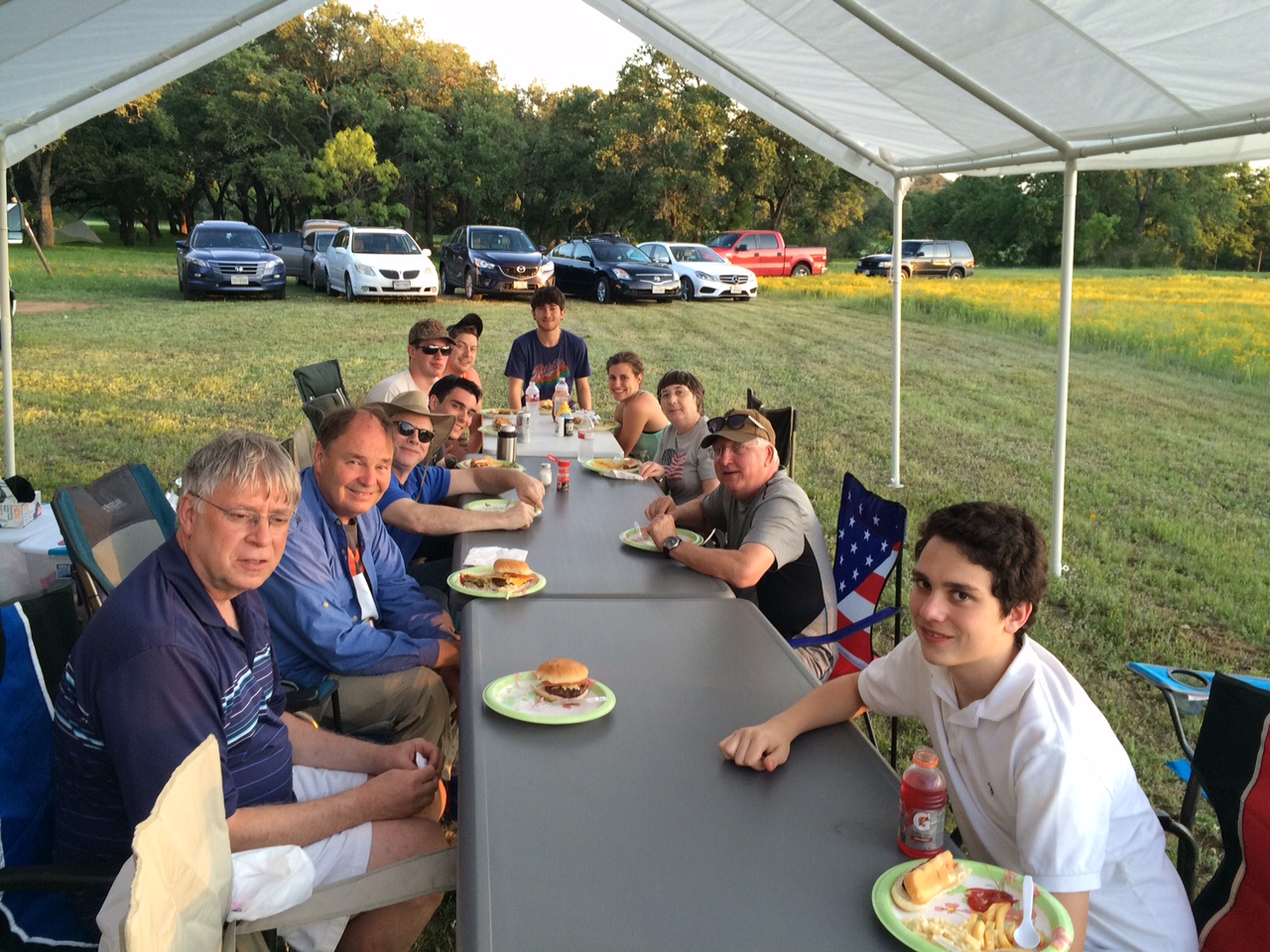
Tekmos Fall Camping Adventure
|
||
| Thank You for Reading Tekmos Talks | ||
|
Thank you for reading Tekmos Talks and helping us celebrate 20 plus years. Sincerely, Lynn Reed, President
|
||
|
|
||
| A Newsletter for the Semiconductor Industry | ||
| November 2016 | ||
| Greetings! | ||
|
Welcome to Tekmos Talks November 2016. This month we will talk more about FPGA Conversions, talk about Tekmos' Temperature Forcing Probe, talk about creating an ad for EE Times and introduce an intern. |
||
| From the Desk of the President, Lynn Reed | ||
|
Block RAM Design-Part 1 Specifications This is the first of a series of articles documenting the design of a dual port, programmable mode, 18K RAM for use in FPGA replacements. Other articles will cover the bit design, word drivers, sense amps, and the timing generator. The first step in any design process is determining the specifications of what you are to design. In leading edge memory design, the choice is obvious. Take what you did before, multiply the size by 4, and you have your new specifications. For most custom RAM applications, memory compilers produce a perfectly acceptable result. You specify the memory size, and how wide each word is, the desired speed, the desired process, and run the compiler. You can be done within minutes. In our case, we need a block RAM whose size can be programmed at personalization, and could even be changed by the user in their application. To get that type of flexibility, we must design our own RAM. Since our customers will have already been using block RAMs in their FPGA based designs, our research starts with determining what the FPGA providers are doing. What are their block RAM sizes? What modes do they support? Are any of those modes covered by patents? Do I have to include the mode in the RAM design, or can I allow the customer to add that functionality in the form of a wrapper around the RAM built out of logic gates? Fortunately, the FPGA companies have provided a wealth of technical information about their block RAMs and their operating modes. After reviewing everything, we decided to create a block RAM that looks a lot like the Xilinx 18K block RAM. This article will discuss the design as implemented in our 180nm process. While the core voltage in the 180nm process is nominally 1.8 volts, we have specified our RAM to also work with core voltages of 1.5 and 1.2 volts. We are looking more for functionality than for speed at the lower voltages. The next article will discuss the bit design. |
||
| Temperature Forcing Probe | ||
|
Tekmos Temperature Forcing Probe
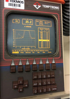
One issue with the probe is that it will also heat the tester that holds the part. We have learned that the best solution is to use a small extender cable so that the part under test is not directly on the tester. In those cases, where the part must be on the tester, we use sheets of thermal rubber as a top insulator, and then put multiple layers of cardboard under that to protect the tester from overheating. We tried ceramic tiles at one point for the underlying insulation, under the belief that if they worked for the space shuttle, then they would work for us as well. But they did not work as well as the cardboard, and so that is what we use. The temperature forcing probe is a strong asset allowing us to provide a superior product for our customers.
|
||
| Tekmos Ad on EE Times | ||
|
Check out our new ad on EE Times For most of November, Tekmos is running a leaderboard ad on EETimes. This ad showcases our new FPGA conversion capability in which Tekmos is offering a reduced NRE if the design fits on one of our existing gate arrays. This ad compliments other ads we are currently running under Google AdWords. This particular advertising campaign is attracting a lot of interest. Not only are we seeing a higher number of clicks, but the CTR (Click Through Rate) is running in the 2% range, which is double the rate we see on other advertising campaigns. This also marks the first time we have used leaderboard (banner) ads, and represents an experiment for us. Many, if not most, engineers use ad-blocking software that is effective at suppressing leaderboard ads. Thus, we had an internal debate as to the effectiveness of such an approach. And being engineers, we decided that the best way to determine effectiveness was to run an experiment. In a month, we will review the results, and modify our ad campaigns accordingly. |
||
| Inside Tekmos | ||
|
Meet Intern Jaime Perez
I have been at Tekmos since September 21, 2016. I informed Kelsey Mehlhorn that I was interested in working in the semiconductor industry. She then referred me to her boss, Lynn Reed, who offered me the opportunity I have now. What are your responsibilities here at Tekmos? My current responsibilities are to support senior engineering with characterization of cell libraries at Tekmos. What are your favorite tasks or projects to work on here at Tekmos? My favorite task is the current one that I am working on at the moment, providing support and learning. What project are you working on now? Since I have only been at Tekmos for a little under two months, I have not had the opportunity to take on multiple projects just yet but I am currently making the transition from logic simulation to IC layouts. Please tell us about your professional and educational background. I am from Edinburg, TX and a Senior at Texas State University. I have a 3.0 GPA majoring in Electrical Engineering with a focus on Micro and Nano Systems and a minor in Applied Mathematics. Prior to Tekmos I was working as a Part-Time Sales Associate at The North Face Outlet and as an employee at Texas State Tubes working on the environmental safety of the San Marcos River. During my down time, I enjoy working out, playing tennis, being outdoors, and spending time with my friends and family in the area.
|
||
| Thank You for Reading Tekmos Talks | ||
|
Thank you for reading Tekmos Talks and helping us celebrate 20 plus years. Sincerely, Lynn Reed, President
|
||
|
|
||
| A Newsletter for the Semiconductor Industry | ||
| October 2016 | ||
|
Welcome to Tekmos Talks October 2016. This month we will talk about Reducing the ASIC NRE, Tekmos' BSI Quality Surveillance Assessment, and talk about Tekmos' 600 Mil DIP Handler. |
||
| From the Desk of the President, Lynn Reed | ||
|
Reducing the ASIC NRE The biggest obstacle to making an ASIC is the initial NRE charge. And the biggest portion of the NRE charge is the cost of the masks. And while the mask charges tend to decline with time, it is still a large number that doubles with each generation of technology node. That being said, there are ways of reducing the mask costs for a given ASIC.
Shuttle RunsThe most widely known method of mask cost reduction is shuttle runs. A shuttle run divides the mask cost among several customers. A mask generally exposes a 20 x 20 mm area. This is divided up into smaller areas, typically being 5 x 5 mm squares. Each square is sold to different customers. The fab combines all of the data bases onto a single mask set, and makes a wafer run. When the run is complete, each customer receives 1 wafer, which will produce from 50 to 100 raw die, depending of the wafer size. A shuttle run will cost about 1/8th of the combined cost of a mask set and one wafer lot. There are several disadvantages to the shuttle run. The first is time. Your design may have to wait one to two months to get on the next available shuttle. The shuttle processing time is also longer than a normal wafer run in that it has to go through all process options. Your design may not use MIM capacitors, but the shuttle lot will go through those steps. The total time for a shuttle run, including the queue time, is about 4 months. A second disadvantage is that you will eventually have to purchase a mask set. The shuttle run will only produce about 50 parts. And while additional shuttle wafers can be purchased, the total available quantities are less than a few hundred. So the shuttle really serves as a low cost Rev A, which must be followed by the high cost Rev B.
MLM MasksAnother approach to mask reduction is Multi-Level Masks (MLM). In this approach, the area of the reticle is divided up into 4 areas. A specific mask layer is put into each section, resulting in an overall mask cost reduction of 75%. Actually, the cost savings are less, since different mask layers have different resolutions, and therefore different costs. The disadvantage is that since the mask area for a given layer has been reduced by 75%, it takes 4 times longer to expose a wafer. And that translates into a higher wafer cost. It also affects fab capacity, and so MLM masks may not be offered by the larger fabs. Economically, there is a point at which the increase in wafer cost equals the cost for a production mask set. We reach this point at about 35 wafers. With a medium sized circuit of 5x5 mm, that translates into a 35,000 unit order. At volumes below this point, MLMs are the best approach. Above that point, a full mask set is better.
|
||
| Reducing the ASIC NRE continued... | ||
|
Gate Array Architectures Our 180 nm basic process has 24 mask layers. By using a gate array architecture for the digital logic and analog circuitry, it is possible to program a gate array with 3 to 4 metal layers, or 6 to 8 masks, counting the vias. Using an existing gate array reduces the mask cost by 66% to 75%. This puts the cost of the programming layers for a gate array on par with the costs for a shuttle run. Another way of looking at this is to note that the costs of a shuttle run followed by a full mask set is comparable to the costs of a full mask set, followed by a programming layer revision, if necessary. And this approach can be much faster than a shuttle run. A shuttle run can take four months, while a gate array can be started before the final design is done, allowing wafers to be held at the first programming layer. So a gate array cycle can be 3 to 4 weeks, instead of 4 months. In many cases, Tekmos may already have base wafers. For example, we have a base array with multiple block RAMs, clock modules, 256 pins, and a SERDES. If the customer design fits in this base, then the programming layers are the only masks that have to be purchased, resulting in a substantially lower NRE.
Design MergesAn approach for a customer with multiple designs is to merge the designs into a single circuit, and implement that as an ASIC. Each design can be activated as a bond option during assembly, and operate as a stand-alone chip. This approach shares the mask costs over several design, without the production die cost penalties associated with a shuttle run. Design merges are complicated. When they share pins, you have to address potential conflicts between output strengths and input levels. Supply pins add a further complication. And it is essential that the circuit that is disabled not draw power when the other design is enabled. We joke that every semiconductor company has tried design merges, and every one of them has sworn to never do it again. But in our case, we have solved the problems, and regularly use design merges. This drawing shows a merge of 4 designs on a single die.
SummaryMasks are expensive. But there are creative design and layout approaches that can substantially reduce them. Talk with us to find out how Tekmos can reduce your NRE costs. |
||
| From the Desk of Director of Operations, Jon Gehm | ||
|
BSI Quality at Tekmos
"Discipline is the bridge between goals and accomplishment." Jim Rohn In life, there is constant, ongoing challenge. These challenges can take many forms. We see examples of this in nature, with the frenetic competitive energy of an ecosystem, bubbling with all forms of life in constant struggle. Or we can find examples in the daily lives of ordinary people, tasking themselves with reasons to strive. For some, these tasks may be to simply work to provide for basic needs. For others, they may find the challenges of life filled with personal objectives, such as improving oneself with knowledge, or pushing themselves to improve a specific physical ability. Whatever the challenge or goal is, there seems to be one constant to make that goal a reality. That is the drive and determination to stay on a task, to see the objective before you, and to move toward that objective with fierce determination. However lowly or lofty the goal, and whether rushing forward or stumbling and plodding, the march must not stop. It is the persistence itself which often wins the day. And as Jim Rohn points out so simply, discipline is the glue that pulls the goal together with the achievement. A business is no different, or any system within that business. To set the goal, then to make the goal real can only be done with the discipline of effort. When a process is evaluated, what is truly being observed, what is truly being measured, is the simple day to day discipline needed to reach the goal of that process. At Tekmos, we recently went through our BSI Quality surveillance assessment, to verify that our Quality Management System was functioning as represented. We found that indeed, our processes and procedures were functioning as they should. But the real achievement was the opportunity to see that the discipline, the bridge if you will, was in place and moving toward our goals. Our goals are customer driven. And it is good to see that at Tekmos, we have a sturdy, though well-traveled bridge, to bring our customers goals to full achievement. |
||
| Inside Tekmos | ||
|
Tekmos DIP Handler
40-pin DIP packages are a very old package design, dating from back in the 70's. They are not very popular, and are not supported by modern handlers. So our only choice was to go to the second hand market, and hope for the best.
As you can see in the pictures, it is strange looking machine, but in excellent shape. It did take us a little while to bring it up. The on-board diagnostics were all in German, which none of us speak. Fortunately, the Google translate app in our phones came to the rescue, and allowed us to communicate with the handler. Our only problem was that it tended to throw empty part tubes around. After a few adjustments, the tubes wound up in the correct holding bin, and we have had no other problems. |
||
| Thank You for Reading Tekmos Talks | ||
|
Thank you for reading Tekmos Talks and helping us celebrate 20 plus years. Sincerely, Lynn Reed, President
|
||
|
|
||
| A Newsletter for the Semiconductor Industry | ||
| September 2016 | ||
|
Welcome to Tekmos Talks September 2016. This month we will talk about Adding Flash to ASICs, Multiple IoT 's, ASIC Prototypes, and Inside Tekmos Water Adventure. |
||
| From the Desk of the President, Lynn Reed | ||
|
Adding Flash to ASICs Some applications need to combine Flash with an ASIC. Tekmos offers two approaches for doing this. The first approach is to just use a process that supports Flash memories. While this sounds simple, it does introduce manufacturing complexities. Many Flash processes require an additional license for both the Flash process and the Flash IP. This adds to the NRE. Once Flash has been included in the design, there is additional testing that must be done, and this testing must be done at probe. Depending on the size of the flash, it may be necessary to add redundancy to the flash to fix flash defects. And in order to test data retention, it is necessary to write a pattern into the flash, then bake it at high temperature for 24 hours, and then re-probe it to ensure that the data is still there. The probe hardware adds to the NRE costs, while the two-pass probe testing adds to the unit price. On the other hand, the addition of a probe test saves money by improving the final test yield. Whether this is a net benefit depends on the overall yield and the package cost. The question of whether the additional NRE charges are worth the advantages of embedded Flash depends on the unit volume. A second approach to embedded Flash is to purchase a Flash die, and use a stacked die approach in the assembly of the ASIC. This approach has both advantages and disadvantages. The advantage is that you bypass all of the flash manufacturing issues and additional NREs. You can also include large amounts of flash that might not be economically possible in the process node you are using for the rest of your ASIC. And the lack of a Flash NRE allows flash to be economically included in small volume ASICs. The disadvantages are primarily economic. You will have to buy megabytes of Flash, even if you only need a few kilobytes. The assembly cost is a function of the number of bond wires, and the interconnect between the ASIC and the Flash can double the packaging cost. This can be mitigated somewhat by using serial Flash memories which have only 8 connections. Serial Flash memories can be much less expensive than the parallel Flash memories, but they can be harder to use from a design point of view. No matter what your Flash requirements are, Tekmos has an approach that will economically add Flash to your design. |
||
| Multiple IoT's | ||
|
Multiple IoT's
When trying to pin down a precise meaning for the term IoT (Internet of Things), it quickly becomes clear that the acronym has many meanings. This article will partially answer the question. At first, IoT meant things that communicate over the internet. But it was about things, not people reading materials that were designed to be read or listened to over the internet. The term has evolved to mean anything that is connected to the internet. It has seen usage to include any sophisticated electronic device, connected to the internet or not. I personally think this later, all-encompassing meaning renders the term useless. The most useful meaning, although not precise, may be to denote the wide range of electronics that communicate over the internet. Some terminology that can be useful is labeling sub-groups of IoT products. The first is the CIoT, The Consumer Internet of Things. This is the area where everyday people directly interface with IoT products. It includes all the home products, such as control of home lighting, heating, safety, and monitoring. The CIoT also includes wearables, such as monitoring one's vital signs, tracking exercise, a device to locate car keys, and watching a personalized TV attached to one's glasses. It includes answering one's door remotely, monitoring children and pets, and lighting systems and sound systems. Another sub-group is the MIoT, the Machine Internet of Things. This term usually refers to older remote control of machines, such as oil wells, monitoring and controlling traffic, signaling trains and rail switching. It is primarily using the internet to communicate between machines that were previously direct wired or connected with dedicated rf links. Another sub-group is the IIot, the Industrial Internet of Things. This usually refers to industrial applications such as precision control of lathes, industrial robots, process monitoring, process control, industrial data analytics, employee monitoring, plant security, and employee safety. Yet another sub-group is the MIoT, the Mobile Internet of Things, primarily related to vehicles, which may not actually use the internet. Often, some type of rf link is used since data must travel between mobile devices. It includes self-driving cars and trucks. It can include large engine control and sensor communications that may not actually use the internet, such as display of tire pressure while the vehicle is moving. It includes many on board communications systems such as DVD players, radios and on board phone systems. It includes driver warning systems such as drifting out of lane warning and adaptive cruise control. Still another sub-group is MIot the Medical Internet of Things which includes medical devices like the remote monitoring of a patient's heart, home measurement of sleep disorders, the control of diffusion pumps, and the pendant used when a person needs to summon medical assistance when alone. Not only is there a lot of overlap in the sub-groupings of IoT, the same MIoT acronym has three different meanings. The same person may use the term in different ways in one conversation. When discussing IoT, it is important to try to get clarification of the meaning of the term for that particular dialog. |
||
| ASIC Prototypes | ||
|
Two Approaches to ASIC Prototyping There is always a risk that the first pass of an ASIC may not work as intended. This can be a result of a design error, a system integration error, or a marketing error in product definition. With ASIC tooling costs being high, most foundries offer a shuttle service. A shuttle works by putting multiple designs on a mask set. In this way, the mask charges are spread over all of the designs. A mask is typically divided up into 16 5x5mm squares. Each customer also gets 1 wafer, which will contain from 50 to 100 die, depending on if the wafer is 200mm or 300mm in size. Since a wafer lot has 25 wafers in it, customers can buy a limited number of additional wafers if more prototypes are needed. Eventually, the customer must purchase a full mask set for production.
Tekmos New SIP Business Card Shuttle runs have another disadvantage in scheduling. They typically run every 4 to 12 weeks, depending on the process and foundry. Then, if the prototypes are good, the availability of production parts can take another 12 weeks of manufacturing. Most design cycles are behind schedule, and this additional delay can be painful. Tekmos uses a gate array architecture on most of its designs, and that allows another alternative to risk management. In a gate array, the circuit size is generally known at the start. And gate arrays have a utilization factor, so a gate array is typically set at 30% larger than needed for a given design. This allows us to start the wafers prior to the design being complete. That alone can cut 3-4 weeks off of the prototype cycle. When the design is complete, we complete the programming layers for the gate array, and complete the prototype process. In the event that the design doesn't work, we have to change the programming layers. Depending on the part, the design will have 3 to 4 programming layers, which is 6 to 8 masks. Since the chip contains from 25 to 27 masking layers, a revision increases the mask costs by 24% to 30%. This compares to a 6% increase in mask costs for using a shuttle run. While at first, the advantage belongs to the shuttle runs, the reality is not so clear. Most digital parts do not need a revision. If fewer than 25% of the parts need a revision, the economics change to favor the gate array approach. And the schedule improvements are more dramatic. If no revision is required, then 3 to 4 months is removed from the production schedule. And time is frequently much more valuable than mask costs. Our gate arrays are frequently designed to meet the requirements of a specific customer. In addition to raw gates, the layout may include embedded RAM, Flash, and mixed signal circuitry. Still, we are frequently able to re-use a given base array for a second customer. In that case, the economics strongly shift over to a gate array approach over a shuttle run. Every case has different economic considerations, and there are many cases where shuttle runs hold a clear advantage. Here at Tekmos, we consider all of these choice to make the most cost effective offering for our customers. |
||
| Inside Tekmos | ||
|
Tekmos River Expedition 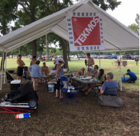
The San Marcos river is a spring fed river that starts in downtown San Marcos. The water is cold and clear. A Texas experience is to get an inner tube and float down the river for a mile. At that point, there was an old dam on the river that the city turned into three spillways and created a water park adjacent to the Rio Vista city park. It is perfect for a company outing. We planned ahead, and some of us arrived early to reserve park space, and erect our tent. The tent came in handy, because it rained for an hour right after we set it up. Leaving behind a cook, the rest of us went to the drop-off point, rented tubes, and floated down the river. The rain had stopped, so it was quite nice on the river. The rain had also kept others away, so the river was not crowded. When we reached the water park, we caught a shuttle back upstream and did it again. Spending two hours floating down a river while stuck in an inner tube is actually tiring. Planning ahead, we had set up a lunch with hamburgers, hot dogs, fries, macaroni and cheese, chips, dips, and brownies. With a menu like that, there was no problem in getting everyone off the river and over to the tent. We ate until no one could walk. Or swim. Then we folded the tent, and called it a day. We did not get any river pictures, but we did get one of lunch. |
||
| Thank You for Reading Tekmos Talks | ||
|
Thank you for reading Tekmos Talks and helping us celebrate 20 plus years. Sincerely, Lynn Reed, President
|
||
|
|
||||||||||||||||||||||||||||||||||
| A Newsletter for the Semiconductor Industry | ||||||||||||||||||||||||||||||||||
| August 2016 | ||||||||||||||||||||||||||||||||||
|
Welcome to Tekmos Talks August 2016. This month we will talk about choosing an affordable ASIC technology, IoT Wearables and our new System In a Package artwork for Unify. |
||||||||||||||||||||||||||||||||||
| From the Desk of the President, Lynn Reed | ||||||||||||||||||||||||||||||||||
|
Choosing An Affordable ASIC Technology Production ASIC technology nodes range from 16nm up to 600nm, and the 10nm and 7nm nodes are nearing production status. With each decreasing technology node, in rough terms, the NRE doubles, the logic density doubles, and the wafer cost increases by ~25%. Going to a more advanced note can result in a cost savings as long as the volume compensates for the increased NREs. There are two items that work against migrating to a more advanced node. The first is the anticipated production volume. Economically speaking, this can be phrased as how many production parts does it take before the unit cost savings equals the increase in NRE, and how long will it take to reach the breakeven point? How long it takes to reach that breakeven point is important. A node selection that breaks even in 5 years is not economical. A project that breaks even in a few months is a no-brainer. Typically, an ASIC node selection needs to breakeven in under a year, with a 6 to 9 month period being ideal. A second point to consider is that an increase in logic density at a given node does not always result in a lower cost die. A die consists of core logic that is surrounded by a pad ring that consists of the input / output buffers, the power bussing, and the scribe line (the space required to allow the die to be cut from the wafer). The I/O buffers have a minimum size that is necessary to withstand ESD damage. The pads have a minimum size because of assembly constraints. And together, this produces a pad ring that does not change size with differing technologies. Consider the case of a 256 pin circuit with a 50u pad pitch. This die will be a minimum of 3.5 mm / side, and have a core area of 6.25mm2. This tables show how many gates can be put into that 6.25 mm2 space. So if a design has less than 400,000 gates, and if the 180 nm node will support the speed requirements, then there is no reason to use a smaller technology node.
Is 400K gates enough for an ASIC? While there are ASICs that routinely exceed that number, especially in the DSP area, there are a lot of applications in which 400K gates are more than adequate. In 2016, less than 20% of our quotes have been for more than 400K gates. And this is for a 256 pin circuit. A 500 pin circuit will have a core area of 39 mm2, and that will hold 2.5M gates. Pad limited designs always go to the least expensive technology node. But what about a non-pad limited design? Consider the case of a 2M gate design. Again, I assume a 256 pin package, and a speed performance that allows a 180 nm implementation.
As this example shows, the most cost effective solution for volumes of under 100K is the 180nm choice. The above statements qualified were by saying that a 180nm process could support the speed requirements. We did so because there are application that do require high speed. A DDR4 interface will need 65nm. A PCI-e Gen 4 will need 28nm. And in those cases, the design mist use the smaller nodes. But in most cases, the most economical node is in the 110nm to 180nm range. |
||||||||||||||||||||||||||||||||||
| IoT Wearables | ||||||||||||||||||||||||||||||||||
|
IoT Wearables
A rapidly growing IoT area is IoT Wearables. Most people who are interested in sports, fitness, new electronic gadgets, or just observant have noticed the Fitbit. It is advertised a lot on Amazon. There are a wide variety of Fitbit products but they are certainly not the only maker of these electronic wristbands. If one stops to think about wearing electronics, you realize it is not a new concept. The comic character Dick Tracy had a wiz bang wrist watch over 50 years ago. And it was connected to other remote devices too. What is different now is that these devices are real and available to anyone at a somewhat reasonable price. Another major difference from the past is that the connection to the internet opens up access from a device to virtually anywhere. Miniaturization of circuitry by technologies, such as Tekmos Unify, is necessary to allow the design of products that are small enough to wear. While most of us have heard about devices such as Google Watch and Google glasses, the types of devices seem limited only by one's imagination. One of my personal favorites if the Fluffy tracker. This is a euphemistic name for a cat tracker that needs to be so small and lightweight that even a five-pound cat has no problem with it on their collar. Of course, it applies to any pet or even livestock. Another app that is intriguing is a wearable that takes thousands of body measurements and then recommends the most flattering clothing to buy online. In mid-July, I went to the Wearables TechCon at the San Jose Convention Center. While not a huge conference, it was an eye opener as to the technologies necessary for wearables. Some products are just good ideas, such as linking a fob on your key chain to your smart phone so that either one can find the other if lost, or inexpensive glasses that show movies and give information. Spinoff ideas such as physiological analytics for analyzing exercise, stress, and recovery go well beyond the hardware to measure and track heartbeat. A similar idea is the real time monitoring of blood chemistry with non-invasive techniques with a wearable on one's arm. The number of companies and products needed to support the wearable products is amazing. Support areas such as flexible circuit boards and plastics to help designing products, testing services, and even universities were all represented at the conference. There were a variety of seminars to increase one's knowledge and awareness of a field that is changing rapidly. A side benefit was an IoT Meet-Up where the main attraction was the demonstration of a set of clothes that could be used to develop natural moving avatars. Although this has been a staple of the imagery in game development, the low price of this product makes it affordable to many individuals rather than just the large game development companies. There are meet-ups on almost any topic, those on technology, especially IoT, are a great way to stay connected and current in a fast changing environment. |
||||||||||||||||||||||||||||||||||
| Inside Tekmos | ||||||||||||||||||||||||||||||||||
|
Unify Graphics The concept behind a Unify SiP (System in a Package) is to stack die within a package using a Tekmos ASIC to include additional functionality and resolve testing and interconnect issues. Because this is a new approach to high density circuits, many are unaware of the details. This requires us to explain it through brochures and other marketing material.
Tekmos New SIP Business Card The first step is to create a drawing that shows how everything fits together. We normally allow our outside artists considerable leeway in how they do our graphics. But in this case, we had to get it to be technically right. We asked our artist to draw a 4 chip Unify SiP, with our ASIC, a processor that was attached via flip-chip, an RF chip, and topped off with a MEMS. You can see the completed artwork below. We are going to use the artwork in a Unify brochure, on a business card sized brochure with a real chip for reference, and on our trade show booth. Normally, images are drawn, which makes them hard to modify. We also asked our designer to create this image using 3-D Adobe software. This allowed us to make multiple changes in how the die were stacked and the relative sizes of the die. And it leaves the door open to future efforts to animate the drawing so that we can show how the die go together. We plan for the animation to be in the form of an animated GIF for the web, an animated PowerPoint slide, and perhaps a short video. And that's the background on our new Unify artwork. |
||||||||||||||||||||||||||||||||||
| Inside Tekmos | ||||||||||||||||||||||||||||||||||
|
Meet Tekmos Summer Intern 
How long have you been at Tekmos and what brought you here? I have been at Tekmos for 7 weeks now. I was introduced to Tekmos by the owner's son, Alan Reed. I have always wanted to learn more about the semiconductor industry. What are your responsibilities here at Tekmos? I am responsible for the repair and maintenance of many machines on the test floor. I have also helped with the wafer nitrogen storage. What are your favorite tasks or projects to work on here at Tekmos? My favorite project so far is working on our laser engraver or Lightwriter SPE. What project are you working on now? I am still currently working on the Lightwriter SPE. Please tell us about your professional and educational background. I went to Westlake High school and I am currently attending Texas A&M, majoring in Civil Engineering. Previously, I was interning for Texas Transportation Institute where I helped build a bridge for testing nondestructive equipment. I worked there for roughly a year. |
||||||||||||||||||||||||||||||||||
| Thank You for Reading Tekmos Talks | ||||||||||||||||||||||||||||||||||
|
Thank you for reading Tekmos Talks and helping us celebrate 20 plus years. Sincerely, Lynn Reed, President
|
||||||||||||||||||||||||||||||||||
|
|
||
| A Newsletter for the Semiconductor Industry | ||
| July 2016 | ||
|
Welcome to Tekmos Talks July 2016. This month we will talk about choosing the right technology and Unify, share that IoT is Not Just for Tech Companies, Inside Tekmos, and the launch of new product TK68HC705C9A. |
||
| From the Desk of the President, Lynn Reed | ||
|
Choosing the Right Technology Node for Your ASIC There are many technology nodes available today, ranging from the most advanced 16 nm up through 1 u. So which one should you use for your ASIC? The answer depends on a combination of circuit size, speed requirements, and production volumes. The biggest downside for the advanced technology nodes is the cost of the masks necessary to fabricate the wafers. The mask cost tends to double for each successive technology node, and is in the millions of dollars for the most advanced nodes. The manufacturing cycle is also longer for the more advanced nodes. The advanced nodes offer greater circuit density, with the density roughly doubling for each node. This reduces the manufacturing costs, but are the savings worth the extra NRE charges? And there is the issue of circuit speed. A DDR4 interface needs at least 65 nm for implementation. A PCIe G3 needs 28 nm. And a mixed signal part can be successfully implemented at 180nm or less. The application sets a lower limit on the technology node. So how do you determine the optimum node? First, let the speed set the lower limit. And trade off the manufacturing cost versus the NRE cost for your anticipated volume. As a rough rule of thumb, the manufacturing savings should pay for the increase in NRE charges within 6 months. Tekmos has pioneered the use of stacked die in an ASIC. Our idea is that you can purchase much of the IP such as processors and RF modules in die form, and use the ASIC for the rest of the system and to interconnect the other die. A huge advantage of this approach is that you can reduce the technology requirements for the ASIC since the purchased IP contains the functions that require the advanced technology nodes. We worked an application that required a DSP function, high speed ADC and DACs, and a processor with large amounts of Flash and RAM. A single chip implementation would require a 28 nm process and the licensing of multiple IP blocks. Instead, we could offer a 180 nm solution with a million-dollar reduction in the NRE. ASICs have a deserved reputation for being expensive. But they don't have to be. Analyzing your application and making intelligent decisions can reduce your costs and produce a superior product. |
||
| IoT | ||
|
IoT is Not Just for Tech Companies Many Technology companies are spending significant money and the attention of high level managers. There are so many conferences and symposiums that one could make attending them a full time job. The need to stay current on developments is not limited to high tech companies. This article addresses one aspect of the Innovator's dilemma for companies that are not in the forefront of innovation. The need to be aware of the developments in IoT is much greater than many companies realize. If part of your company makes garden variety electrical products, such as doorbells, you may wake up to the fact that companies, such as Ring, are making devices that let the homeowner see who is at the door on their smart phone, wherever they are. While these devices may be pricey now, it is the way things are going. Many people remember when Kodak was almost the only name most people knew regarding taking family photographs. Of course, Polaroid was the name if one wanted the print almost immediately. Many young people do not even recognize these companies' names now. Business classes will probably study these cases and have opinions whether the companies could have adapted to the changing times better than they did. Are sump pump manufacturers watching for the best time to have links to smart phones? What if your company has never considered having your sump pump send a text to the homeowner when the backup battery is low or about to fail? By the time you start developing a product to match your competition, they may have already made significant inroads to your market share. There is no precise definition of IoT. Many consider it to include devices which may not actually be connected to the web. Self-driving cars and trucks are examples. The large manufacturers of cars and trucks seem to be closely attuned to technology advances but even that is not clear. Detroit was caught off guard when Japanese cars started to eat their market share. It will not be that long before self-driving cars are commonplace. One wonders if the changes in technology are really being tracked by all the supporting companies that supply both OEM companies and after-market companies. Today there are cars that can parallel park themselves. Which companies will lose market share when they are behind in making the electronics and software to let you summon your car from the parking lot to the mall entrance? It is not hard to imagine using Uber to get a ride and find that the car you summoned does not have a driver. If your company makes after-market parts for cars, you must keep up with the trends in retrofitting or have your competition steal your customers. With the rate of change itself accelerating, companies that might even remotely be touched by IoT must be aware of developments. By the time a company should take action, it will likely be too late to start to develop plans. Any company who thinks IoT will not affect them, takes this position at their own risk. |
||
| New Product Announcement | ||
|
The TK68HC705C9A Tekmos has expanded its line of microcontrollers with the introduction of replacements for the NXP (Freescale) MC68HC705C8A and MC68HC705C9A microcontrollers. The TK68HC705C9A is an 8-bit microcontroller with the following features:
The Tekmos TK68HC705C9A also has a configuration register that allows the part to be re-configured to replace both the MC68HC705C8A and the MC68HC705C12A. An interesting feature of the configuration register is that it changes the physical pinout of the TK68HC705C9A to match the pinout of the MC68HC705C8A. The TK68HC705C9A uses Flash to replace the original EPROM program storage. This means that while the original parts were OTP (One Time Programmable), the Tekmos version is fully re-programmable. The TK68HC05C9A is a ROM version of the part that provides a low cost solution for high volume production. Both the TK68HC705C8A and TK68HC705C9A are available in the 44-pin PLCC (FN), 40-pin PDIP (P) and space saving 44-pin PQFP (FB) packages. |
||
| Inside Tekmos | ||
|
Tekmos Eagle Scouts
Tekmos has the unique distinction of having Eagle Scouts and family members of Eagle Scouts among its ranks, including the founder and president, Lynn Reed. Eagle Scout is the highest rank attainable in the Boy Scout program of the Boy Scouts of America (BSA). Eagle Scout Tekmos Team Members include Vema, Will, Clay, Alan, Adrian and Vishnu, along with Lynn Reed. Vema says "Scouting was a good time to practice leadership. As a Scout I found through camping in cold, rainy weather I had to get out of my comfort zone. All of my experiences in Scouts prepared me for real life." When Will was asked about his experiences he stated, "I learned about the world, how to organize, about fundraising, how to get along with others, and being an Eagle Scout influenced who I am today as well as got me this job." Clay, a junior in college who has worked several summers at Tekmos says, "Scouts helped me gain friendships I can count on and made me more aware of putting others needs before mine." Alan works full time at Tekmos now, but worked summers and breaks while in school. "I learned a sense of leadership and management particularly creating my Eagle Scout project where one has to plan everything in advance and then be completely removed from the equation so that the project can be implemented. It was my first experience with managing and leadership from afar." Adrian, the testing floor manager, says of his Scout experiences, "Scouting has been a good way of life. It has provided me with the tools for leadership to take on any obstacle and be successful." Adrian earned all 121 merit badges in 2007, the first to earn that distinction in Central Texas. He held that position for close to 10 years. Vishnu, a recent graduate from college, will be leaving to join the military. "Scouts gave me the confidence to get up in front of people, give orders, and direct. I also learned to accept when I was wrong and take advice." Other Tekmos Team members associated with Boy Scouts are Carole Reed, who serves as the Capitol Area Council Advancement Chair for the greater Austin area. She began volunteering when her sons were in Cub Scouts and finds it rewarding to watch the young boys grow to such fine young men from their scouting experiencing. Jon Gehm and Renee Dalton each have sons in scouting and both volunteer with their son's troops. Rick Holman served as a troop leader. All have volunteered in leadership positions. The first Scout to earn the highest rank of Eagle Scout was Arthur Rose Eldred, a member of Troop 1 in Oceanside, New York, a troop his brother Hubert had founded in November 1910. The younger Eldred earned his 21st merit badge in April 1912 at the age of 16. Since there were no provisions for local reviews in those early days, Eldred was examined by perhaps the most exalted and intimidating board of review in Scouting history: Chief Scout Executive James E. West, Chief Scout Ernest Thompson Seton, National Scout Commissioner Daniel Carter Beard (another BSA founder), and Wilbert E. Longfellow of the U.S. Volunteer Life Saving Corps, who had written the Handbook's sections on swimming and lifesaving. National Eagle Scout Association 2008 Eagle Scout Directory. |
||
| Thank You for Reading Tekmos Talks | ||
|
Thank you for reading Tekmos Talks and helping us celebrate 20 plus years. Sincerely, Lynn Reed, President
|
||
|
|
||
| A Newsletter for the Semiconductor Industry | ||
| June 2016 | ||
|
Welcome to Tekmos Talks June 2016. This month we will share about being a corporate sponsor and exhibiting at HiTEC 2016, May 10-12 in Albuquerque, NM., and exhibiting at IoT Devcon May 25-26 in Santa Clara, Ca. We are very pleased to launch new product TK87C752 Microcontroller. |
||
| From the Desk of the President, Lynn Reed | ||
|
New Product Announcement Tekmos now offers the TK87C752 Microcontroller as the latest addition to the Tekmos TK8xCx51 family of microcontrollers. The TK87C752 can be used as a drop-in replacement for the 87C752 that many manufacturers are having trouble locating due to discontinuance by other component suppliers. The TK87C752 is an enhancement of the TK87C51 and re-packaged in a space saving package. The 87C752 contains 256 bytes of RAM, 64K bytes of Flash memory, 21 I/O lines, a five channel, 8-bit ADC, a 16-bit auto-reload counter/timer, a five-source, fixed-priority level interrupt controller, an I2C interface, an 8-bit PWM output and an on-chip oscillator. Like other members of the TK8xCx51 family, the fully static design of the TK87C752 allows operation at frequencies from DC to 16 MHz. It is a low power device with an Idle mode and a Power-Down mode for even lower current. Detailed specifications including block diagrams, electrical specifications, and timing diagrams can be found in the Tekmos TK87C752data-sheet. The TK87C752 microcontroller is currently available in plastic 28 -pin PLCC and 24-pin PDIP packages. Having a drop-in replacement for parts has shown to be a very cost effective way to extend the life of products when the original component manufacturer discontinues a part. The availability of a drop-in replacement part eliminates the need to make the tough decision whether to redesign a printed circuit board or discontinue a product. Tekmos continues to be the "go to" supplier when there are problems finding obsolete parts or when additional parts are needed after the date for EOL (End of Life) purchase has passed. Tekmos makes a variety of microcontrollers, microprocessors, and other miscellaneous standard products to satisfy these needs. Tekmos also continues to make custom ASIC replacement parts. Customers are aware that buying from Tekmos ensures pin for pin, drop-in replacements that can be counted on to work in their applications, without worry about the quality of parts purchased on the grey market. |
||
| HiTEC 2016 | ||
|
International Conference on High Temperature Electronics (HiTEC 2016)
On the second week of May, Lynn Reed, Bob Abrams, and Richard Stallkamp went to the HiTEC Conference in Albuquerque, New Mexico. HiTec is dedicated to high temperature electronics. While there are many applications that require electronics to work at high temperatures, the largest commercial usage has been in the oil industry. Oil exploration is a very expensive endeavor. Being able to put electronics deep underground is necessary in order to determine what is going on a couple miles down where it is quite hot, perhaps 200ºC to 300ºC. The lifetime of electronics can be quite short under these harsh conditions. Tekmos has introduced several state of the art products that are rated at 250ºC with proven operation to over 300ºC (570ºF). There are applications that also require high temperatures, such as geothermal. Generally, designers make trade-offs between the highest operating temperature and cost. Silicon based parts seem to offer the best trade-off for oil exploration applications. The Tekmos approach can offer the best trade-off because it is silicon based and at the high end of temperatures which can be achieved with silicon. Unfortunately, oil exploration is in quite a slump because of the lower price of oil. The attendance at the conference was down significantly from prior years due to current economic conditions. The conference was still successful because it is the quality of the contacts made that is important, not the quantity. |
||
| IoT Devcon 2016 Conference | ||
|
Internet of Things: Connecting Things, People & the World
There are so many aspects of IoT (Internet of Things), that one can hardly list all the topics and issues. The number of IoT conferences these days is so large that one could just about go to one every week. Tekmos decided that one conference we really wanted to take in this year was the Internet of Things Developers Conference held May 25 and May 26 in Santa Clara, California. The Unify Program at Tekmos focuses on the ability to unify many chips into a single package. Unify is a methodology, a capability, or a usage of technology, to yield several advantages. The users of the Unify Program are most likely to be the developers of IoT. The best place to describe the Unify Program is face to face with the IoT developers. A short definition of Unify is the combining of chips from different technologies into a single package using a Tekmos ASIC as the base. It combines sophisticated cutting edge, off-the-shelf, chips that are inexpensive because of their volume, with added circuitry along with a Tekmos ASIC. the Tekmos chip performs like a silicon PCB. By implementing this as the Tekmos chip base with other die stacked above it, issues of mismatch pinouts between the standard parts are solved. This stack of die is in a single package. The small size of the resultant "System in a Package" (SIP) can be important for many IoT products. (Think wearables, such as fitness monitors.)
Other real advantages are cost and time to market. For example, a design with Flash memory and a microcontroller could use highly sophisticated ICs, which are already developed, mounted on a relatively inexpensive customized ASIC built with an older, less expensive technology. A common theme here is only pay for the technology you need in the parts of your system that require it. A high end processor can be mounted on a slower, less expensive technology base. The processor is inexpensive even though it uses cutting edge technology because its volume in the general market is high. This IC is combined with a specialized base ASIC that makes the design very hard to copy. Since 90% of the design implementation as utilizes commercially available parts it so far less risky than building a large expensive complex chip from scratch. As expected, there were a number of conversations with developers that need to have small form factor and low power product designs. We are excited about the future for offering these benefits to many customers. |
||
| Inside Tekmos | ||
|
Hi-TEC 2016 Side Trip
The crowd seemed to be mostly local people enjoying the music, inspiring some of them to dance. After a great Mexican dinner, we went back to the hotel to get ready for the next day, having enjoyed some of the local talent and a chance to get away for a few hours. |
||
| Thank You for Reading Tekmos Talks | ||
|
Thank you for reading Tekmos Talks and helping us celebrate 20 plus years. Sincerely, Lynn Reed, President
|
||
|
|
||
| A Newsletter for the Semiconductor Industry | ||
| May 2016 | ||
|
Welcome to Tekmos Talks May 2016. Tekmos will be a corporate sponsor and exhibiting at HiTEC 2016, May 10-12 in Albuquerque, NM., and exhibiting at IoT Devcon May 25-26 in Santa Clara, Ca. We are pleased to launch new product TK87C750 Microcontroller, to talk about "The Real Cost of ASICs," and share "Inside Tekmos' Enchanted Camp out". |
||
| From the Desk of the President, Lynn Reed | ||
|
New Product Announcement Tekmos now offers the TK87C750 Microcontroller as the latest addition to the Tekmos TK8xCx51 family of microcontrollers. The TK87C750 can be used as a drop-in replacement for the 87C750 that many manufacturers are having trouble locating due to discontinuance by other component suppliers. The TK87C750 is a subset of the TK87C51 and re-packaged in a space saving package. The 87C750 contains 256 bytes of RAM, 64K bytes of Flash memory, 19 I/O lines, a 16-bit auto-reload counter/timer, a five-source,fixed-priority level interrupt controller, and an on-chip oscillator. Like other members of the TK8xCx51 family, the fully static design of the TK87C750 allows operation at frequencies from DC to 16 MHz. It is a low power device with an Idle mode and a Power-Down mode for even lower current. Detailed specifications including block diagrams, electrical specifications, and timing diagrams can be found in the Tekmos TK87C750 data-sheet. The TK87C750 microcontroller is currently available in plastic 28 -pin PLCC and 24-pin PDIP packages. Having a drop-in replacement for parts has shown to be a very cost effective way to extend the life of products when the original component manufacturer discontinues a part. The availability of a drop-in replacement part eliminates the need to make the tough decision whether to redesign a printed circuit board or discontinue a product. |
||
| ASICs | ||
|
The Real Cost of ASICs It is widely believed that an ASIC will always cost at least a million dollars. There are certainly real life examples of ASICs costing that much. That does not mean they all have to. The real cost can be as low as $50k to $250k. Tekmos has certainly made customized gate arrays that have cost less than $100k. The first issue in controlling cost is picking the technology you need. Each smaller technology node is more expensive than the previous, larger technology. While it may be exciting to use state-of-the-art, latest, greatest, and smallest geometry technology, it can be a colossal waste of money if the speeds or densities are not really required. While it might be fun to drive a Lamborghini to church on Sunday, there are certainly less expensive ways of getting there. In addition to the engineering design, the total cost of producing an ASIC is the NRE plus the unit cost multiplied by the number of units. If the volume is very high, unit cost dominates the decision. If projected volume is low, it may be that the tooling/mask cost is the main concern. It is important to remember that it is this total cost that one needs to minimize. There are ways to get small volumes produced that are not as expensive as one might think. Let's talk about multilayer mask sets first. It is possible to have more than one processing layer on a single processing mask. This multi-level mask approach can reduce the total costs for masks by about half at the expense of doubling the wafer processing costs and therefore the unit cost. This presents one with the trade-off problem of estimating the total volume of units required. If only a few thousand parts are needed, it may well warrant the less expense masks at the higher unit cost. Using a smaller geometry often makes a die smaller, resulting in more die per wafer. But the cost of processing each wafer can go up significantly. If the smaller device with its related increase in speed is not needed, using a smaller technology to make a smaller die and get more die on a wafer may actually result in an unnecessary increase in total cost. Minimizing die size may not be the appropriate end goal, minimizing total cost is usually more important. Another consideration in the attempt to reduce cost by creating a smaller die is the need to have enough area associated with each bonding pad. The ESD protection circuitry requires enough area at the periphery to eliminate this source of damage. If the periphery is the limiting factor in determining the dimensions of the die, making the core smaller with smaller technology transistors only increases the cost of the same sized die. Another approach to lowering total cost is using shuttle runs, the sharing the wafer with other designs. Many people are familiar with the way MOSIS can produce small volumes at very modest prices. If the number of die required is small, this can be the most efficient way if getting the processing done. Depending on total volume requirements, it may be appropriate to have the total production done with the shuttle run approach. A combination of these processing techniques can go a long way toward keeping the processing costs of ASICs at a level significantly lower than the million dollars sometimes talked about. |
||
| IoT Devcon 2016 Conference | ||
|
Internet of Things: Connecting Things, People & the World Tekmos looks forward to exhibiting at the Internet of Things Developer's Conference May 25-26 in Santa Clara, California and will feature Tekmos Unify, our solution to the IoT. The Internet of Things (IoT) goes way beyond and interconnects virtually unlimited numbers of smart objects and changes the way we interact with our environment. To help rein in the vast IoT world, the IoT DevCon 2016 will focus on technologies ranging from the ultra-low power microcontrollers to the multicore-enabled aggregation hubs to the software and security infrastructure required for monitoring and management of the enormous bundles of data. Stop by booth #11 to learn more about Tekmos' Unify, ASICs for the Internet of Things.
|
||
| Inside Tekmos | ||
|
Tekmos Enchanted Camp Out Tekmos Team members gathered together for the first time for what hopefully will be a twice annual camp out at Oxford Ranch Campground in Llano, Texas, in the heart of the Texas Hill Country. April in the Texas Hill Country means lots of wildflowers, including the state flower, the bluebonnet, and perfect spring temperatures with many options for hiking, visiting a Presidential home, or wine tasting. 
The afternoon was spent playing card games, relaxing and visiting followed by an evening of great food and music. Tekmos resident chef/cook, Phil Buck prepared an enjoyable dinner consisting of the perfect camp food; hamburgers, hot dogs, barbecue chicken, green beans, caramelized carrots, French fries to rave about, macaroni and cheese followed by s'mores.The rest of the evening we were serenaded by engineer, Rick Holman's strum of the guitar and country/blue lyrics. After a good night sleep in the fresh Hill Country air and a tasty breakfast, some went for a hike to Enchanted Rock for a good stretch of the leg and commune with nature. Others ventured to Fredericksburg for great shopping and home to more than 15 vineyards and wineries. Oxford Ranch Campground 160 acres is located approximately ten miles south of Llano off of State Hwy 16 in the Texas Hill Country. A working cattle ranch offers tent camping under oak trees, bath-house (with hot showers) and also have hiking, mountain biking and trail rides available. This camp is close to one of the starting points for the back roads to Click scenic route if you are interested in exploring the boondocks. RV sites are available and pets are ok if kept on a leash. Enchanted Rock (16710 Ranch Rd 965, Fredericksburg TX) is an enormous pink granite pluton batholith located in the Llano Uplift approximately 17 miles (27 km) north of Fredericksburg, and 24 miles (39 km) south of Llano, Texas. Archaeologists discovered trace of human life back 11,000 years. Folklore of local Tonkawa, Apache and Comanche tribes ascribes magical and spiritual powers to the rock (hence the name 'Enchanted Rock'). "Hill Country" is a vernacular term applied to a region including all or part of twenty-five counties near the geographical center of Texas. It is bordered on the east and south by the Balcones Escarpment, on the west by the relatively un- dissected Edwards Plateau, and on the north by rolling plains and prairies. The elevations range from less than 1000 feet in the south and eastern areas of the Hill Country and generally rise toward the north and west to reach more than 2500 feet. President Lyndon B. Johnson was born near Johnson City. Learn about this colorful Texan at the Lyndon B. Johnson National Historical Park. Tour the Texas White House and Johnson's boyhood home. Drive the Peach Loop, one of TPWD's Great Texas Wildlife Trails. It will lead you to some of the best wildlife observation points in the area. A great time was enjoyed by all with definite plans for another camp out in the fall. |
||
| Tekmos Tidings Corner | ||
|
Tekmos Celebrates Nineteen Years Tekmos celebrates 19 years in business and it's 1st anniversary in our new building at 7901 Riverside, Bldg.2, #105, Austin, TX. location. Tekmos was a featured site of the day April, 29th on EEWeb.com. Tekmos is a sponsor and exhibitor at HiTEC 2016 in Albuquerque, NM May 10-12. Stop by our booth for a visit and to learn more about our high temperature chips. |
||
| Thank You for Reading Tekmos Talks | ||
|
Thank you for reading Tekmos Talks and helping us celebrate 20 plus years. Sincerely, Lynn Reed, President
|
||
|
|
||
| A Newsletter for the Semiconductor Industry | ||
| April 2016 | ||
|
Welcome to Tekmos Talks April 2016. Tekmos will be a corporate sponsor and exhibiting at HiTEC 2016, and exhibiting at IoT Devcon in May. This month we are pleased to announce Tekmos compliance statements for REACH and RoHS in our ongoing green initiative, and to the launch of a new product, the TK87C749 Microcontroller. |
||
| From the Desk of the President, Lynn Reed | ||
|
Tekmos is Conference Bound Tekmos once again is a corporate sponsor and exhibiting at the International Conference on High Temperature Electronics, May 10-12 in Albuquerque, New Mexico and will be exhibiting at the IoT Developers Conference in Santa Clara, California May 25-26. HiTEC is a forum for presenting leading high temperature electronics research results and application requirements and the Iot Devcon is a conference and trade show specifically for the IoT product developer. Tekmos has presented a paper, and maintained a display table at the July 6-8 2015, International Conference and Exhibition on High Temperature Electronics Network at Churchill College in Cambridge, England, at HiTEC 2014 in Albuquerque, and attended earlier conferences. This annual conference, alternates venues between the U.S. and England, is dedicated to high temperature electronics, ranging from the relatively cool 175ºC up to the 1200ºC range for Silicon Carbide. It also covers high temperature materials and passive components. Attending the presentations does a lot more than just give Tekmos an opportunity to present our research. Listening to the presentation of other papers has led to some consideration of additional techniques that Tekmos may pursue. It is important to know what others are doing. The question and answer period following each presentation gives more insight and understanding than can be obtained from reading the paper alone. One advantage of exhibiting at a conference is that it provides feedback about what customers really want to see in products. It also shows what the competition is doing. Together, that provides invaluable marketing guidance for our own efforts. The HiTEC conference is small, with about 300 attendees. We have been to shows that were 30 times larger, and gone away with a fraction of the leads we got from HiTEC. We must always question how Tekmos compares to the competition in all of our offerings including Unify ASICs for the Internet of Things and high temperature chips. These two events will provide that arena to learn more. |
||
| From the Desk of Director of Operations, Jon Gehm | ||
|
Tekmos Achieves REACH & RoHS In Ongoing Green Initiative As children, many people seem to have trouble eating their vegetables. I can still remember my own grandmother's disapproving look, as basically everything but the vegetables disappeared from my plate. Of course I would then make a valiant attempt at dessert, as my grandmother's cobbler, pie or chocolate anything was truly the stuff of legend. But she would have none of it. It was back to the vegetables for me, with dramatic slow, choking swallows, while simulating my best near death experience. In time, to her credit, creativity came to play a role. It was probably the peas, floating in gravy, nestled seductively in a puddle on top of my mash potatoes that started the change. "Ducks in a pond", she called it. Ok, so they weren't ducks, and it was not a pond. But the peas went down quickly, and the whole thing tasted pretty darn good. In time the green beans, carrots and honestly just about anything became fair game. I guess I can blame my grandmother, as today there doesn't seem to be anything that could possibly land on my plate that will not be eaten with great enjoyment. Maybe too much so, if the truth was told. Doing something that may seem to be a problem, to have an eventual better overall outcome, is not just a technique for grandmothers. The rules of an organization, or laws of a land can also be viewed through such a lens. In Europe, for example, the large number of chemical substances being manufactured, and the unknown effect on human health and the environment became a concern. Regulations were created, such a Registration, Evaluation, Authorization and Restriction of Chemicals (REACH), to register, evaluate, authorize and possibly restrict certain harmful chemical substances. Or the Restriction of Hazardous Waste in Electrical & Electronic Equipment (RoHS) directive, where components are tested for specific substances, such as Lead (Pb), Cadmium (Dc), Mercury (Hg) as well as a list of other materials to verify there is less than 0.01% of that substance by weight. While these regulations do require more work and verification, they also truly do help protect the environment and human health. At Tekmos, we take these directives seriously. We take the extra effort needed to help ensure that potentially harmful substances are controlled throughout our industry and in our business practices. Tekmos REACH and RoHS Compliance Statements have been created, and are easy to view and download from our website. We view compliance with these directives as our responsibility and obligation, to our business partners, our employees, and all others who use and depend on the products we make. At Tekmos we take the effort to make our world a little safer. Oh, and we also don't mind eating our vegetables when the time comes either. |
||
| IoT | ||
|
IoT Standards
The excitement that IoT offers great new possibilities to all phases of our lives is beginning to be tempered by the realization that having standards is critical and that agreeing on them takes a herculean effort. Talk to someone who remembers trying to decide between buying a VHS and Betamax VCR. The two video recording/playback formats lived side by side for many years. While each had their own merits, they were not compatible. If you had one you could not use products designed for the other. Incompatible IoT devices is a much larger problem because of the very large number of types of products and companies involved. Virtually all types of consumer products, from home entertainment to home appliances and from automobiles to retail sales can have IoT aspects to them. All manufacturing, commerce, and infrastructure will have some connection to IoT issues. For example, plumbing may seem a long way from any IoT concern, except perhaps in remotely controlling flood gates or remotely monitoring water flow in streams. Consider that a washing machine can detect its own stuck valve and, using IoT, have the water main valve to your home shut off. This may sound far-fetched until one considers that water damage from such occurrences are a major reason for homeowner insurance claims. Without standards, it is unlikely that devices in unusual pairings will be able to communicate with each other. Each potential vendor in the IoT space has an interest in some aspect of the standard. Any standard will likely cause some winners and some losers. Should all communications between devices go through the cloud? It would be far too cumbersome to have everyone's in-home entertainment center communicate through the cloud to dim the lights when movies start. Would there be a master list of all lightbulb serial numbers to know which ones to dim? How will the maker of the light switch dimmer interact with the changes requested by the entertainment system? In this arena, it certainly appears that communications for these devices must be local. This can be contrasted with the wide area issues of coordinating energy sources and users on the power grid. It is difficult to get agreement on standards within a committee when each company participating has their own vested interest in standards favoring their approach. Perhaps worse than that, the number of standards committees is growing. Any major company will likely participate in competing standards committees to follow trends as well as to influence the standards being developed. There seem to be two groups emerging to dominate the discussions: The Open Interconnect Consortium and the Allseen Alliance. Each want to be the single standard for IoT. Not surprisingly, the standards each is moving toward do not necessarily agree with each other. Much will need to happen before there is anything like a single standard. Meanwhile, products are being designed and manufactured which may not function well with designs produced after there is more agreement on standards. |
||
| New Product Announcement | ||
|
Tekmos now offers the TK87C749 Microcontroller as the latest addition to the Tekmos TK8xCx51 family of microcontrollers. The TK87C749 can be used as a drop-in replacement for the 87C749 that many manufacturers are having trouble locating due to discontinuance by other component suppliers. The TK87C749 extends the functionality of the TK87C51 with the addition of a 5-channel, 8-bit ADC, and an 8-bit PWM circuit. Like other members of the TK8xCx51 family, the fully static design of the TK87C479 allows operation at frequencies from DC to 16 MHz. It is a low power device with an Idle mode and a Power-Down mode for even lower current. Detailed specifications including block diagrams, electrical specifications, and timing diagrams can be found in the Tekmos TK87C749 data-sheet. The TK87C749 microcontroller is currently available in plastic 28-pin PLCC and 28-pin PDIP packages. Having a drop-in replacement for parts has shown to be a very cost effective way to extend the life of products when the original component manufacturer discontinues a part. The availability of a drop-in replacement part eliminates the need to make the tough decision whether to redesign a printed circuit board or discontinue a product. Tekmos continues to be the "go to" supplier when there are problems finding obsolete parts or when additional parts are needed after the date for EOL (End of Life) purchase has passed. Tekmos makes a variety of microcontrollers, microprocessors, and other miscellaneous standard products to satisfy these needs. Tekmos also continues to make custom ASIC replacement parts. Customers are aware that buying from Tekmos ensures pin for pin, drop-in replacements that can be counted on to work in their applications, without worry about the quality of parts purchased on the grey market. For more information on Tekmos products contact sales@tekmos.com or call 512-342-9871 |
||
| Thank You for Reading Tekmos Talks | ||
|
Thank you for reading Tekmos Talks and helping us celebrate 20 plus years. Sincerely, Lynn Reed, President
|
||
|
|
| A Newsletter for the Semiconductor Industry |
| March 2016 |
|
Welcome to Tekmos Talks March 2016. |
| From the Desks of the President |
|
Tekmos Unify Brochure Ready for Conference This month we have published our brochure describing Unify ASICs for the IoT. System engineers need to meet the challenges of smaller physical packaging, lower power consumption and better connectivity solutions that offer fast time to market. The Unify - ASICs Brochure describes capabilities and approaches of how Unify ASICs achieve smaller space with low power by using standard parts combined with our low risk Unify ASIC. The Unify ASIC features a silicon interconnect combined with integration of logic and mixed signal technologies by Tekmos for better connectivity solutions. The Unify ASIC designed by Tekmos for the customer, provides a breakthrough approach offering the lowest development cost for a System in a Package solution for new products. The Unify ASIC includes design security making it extremely difficult for others to copy a customer's product design. Unify ASICs protect market share and allow the customer to maintain higher selling prices over the life of their product. Tekmos will be an exhibitor at the upcoming IoT Developers Conference in Santa Clara, May 25-26. We will be located in the exhibit area and look forward to your stopping by to see how Unify ASICs can improve your product developments. The month of May seems to be a great time for many conferences this year. Tekmos is a major sponsor and exhibitor at the upcoming IMAPS HiTEC High Temperature device conference in Albuquerque, New Mexico, May 10-12. Tekmos will be featuring our high temperature microprocessors, memory devices and ASICs, with ASICs able to operate up to 300ºC. We look forward to presenting our latest product offering for high temperature applications ranging from 175ºC to 300ºC. Please visit us in the exhibit area and learn more about our high temperature microprocessors and ASICs with long lasting operational life. If you have any questions, please contact us at: sales@tekmos.com |
| Stacked Die Assembly & Unify |
|
Tekmos Unify ASICs: Stacked Die Assembly Applications for the IoT are driven by several factors including power, development time, and space, denoting a desire for compact packages. Major semiconductor suppliers have developed cost effective blocks to meet about 90% of the required needs. But what about the other 10%? Tekmos has created a cost effective ASIC using an appropriate technology to address that missing 10%. We use stacked die assembly to add the processor, wireless communication, sensor and other standard features resulting in a single chip implementation of your system, giving you the advantages of an ASIC, but without the high NRE charges. Tekmos Unify - ASICs creates that distinctive partnership with your standard building blocks and unique IP. Tekmos' approach of unifying existing parts with a technology appropriate ASIC in a stacked die package is one way to be cost effective. Another way Tekmos offers a way to reduce costs often happens with new product development. It is common for the design to change after its first exposure to the consumer. Tekmos offers the ability to run engineering lots or shuttle runs on the initial silicon. This offers a great way to produce 100s or 1000s of parts without a large investment in photomasks. When the product reaches market acceptance, Tekmos can invest in a full mask set to support high volume and meet lowest cost. For more information about Unify - ASICs, contact sales@tekmos.com |
| Tekmos Unify Design Security |
|
Design Security Let's face it, there are incredible advantage to the IoT, and then there are the drawbacks, specifically security. Many of us deal with one type of security issues on a daily basis from credit card theft to phishing our smart phones and regular spam to our inbox. But what about security of the design itself? Products made from standard parts can and are copied and sold as counterfeit chips. What if the design includes a proprietary ASIC making it more difficult to copy? At Tekmos, the designer can be certain no one else has access to the design or to Unify - ASICs without permission. Tekmos takes pride in its specialized knowledge. Customers only need to define their system in RTL and to have verified their design in a prototype such as an FPGA. We will take it from there and design a product more secure for your customers. For more information about Tekmos' product line, contact sales@tekmos.com ,call 512-342-9871 or fill out our form here. |
| Tekmos Mixed Signal ASICs |
|
A Unify - ASIC from Tekmos can include mixed signal circuitry and Tekmos can add the interface to your design to connect with the outside world. It can be sensor integration, additional power supplies, battery management, or signal conditioning. For example, an application may require connecting a microphone to the system. The microphone needs a biasing circuit, a gain control, and an amplifier so that the full range of the microphone is matched to the ADC. This can be implemented using 10 to 20 discrete components or embedded in a Tekmos mixed signal ASIC. Tekmos uses an approach called structured arrays to implement our mixed signal designs. It provides many advantages. Tekmos may already have an array that we can use for your project, reducing NRE charges. For more information on Tekmos products contact sales@tekmos.com or call 512-342-9871 |
| Thank You for Reading Tekmos Talks |
|
Thank you for reading Tekmos Talks and helping us celebrate 20 plus years. Sincerely, Lynn Reed, President
|
|
|
| A Newsletter for the Semiconductor Industry |
| February 2016 |
|
Welcome to Tekmos Talks February 2016. This month we will share more on Tekmos' UNIFY our answer for the Internet of Things, IoT & Security, talk about doubling Tekmos test capacity, feature Tekmos microprocessors, and share a human interest story. |
| From the Desk of the President, Lynn Reed |
|
Doubling Tekmos Test Capability
Tekmos has just doubled our test capacity, and this is the story behind it. Once you have chosen a brand of testers, there are strong incentives to keep on using that brand. The first is the cost of test hardware. Each part has a dedicated load board. While each hardware set is on the order of a thousand dollars, we do a lot of chips and over time we have hundreds of thousands of dollars invested in test hardware that is dedicated to a specific tester. Another incentive is the software associated with the test programs. We have man-years of engineering time invested in the test programs which would be lost with a new tester brand. That is why we were excited to learn that a major semiconductor foundry was closing their test facility, and selling six of the same brand of tester that we use. Used testers sell at a steep discount, and we got a good purchase price. The main issue was that the testers were in China, and it was our responsibility to get them back to Texas. The first step was to hire a Chinese packing company. Each tester and each manipulator was put in a hermetic bag, and then packed in a custom shipping crate. Then, all 12 crates were packed in a 40 foot shipping container. Andy then made arrangements to have the container shipped from Shanghai to Houston. We knew the name of the ship, and as a result, were able to track it's movements across the Pacific, through the Panama Canal, and on to Houston. The tracking detail was accurate enough that we could see it wait as the locks filled on the canal. Eventually, the container arrived at our warehouse, and we were able to inspect what we have bought. There is always a risk in buying things from overseas, because you only get to look at photographs of the merchandise, and there is never enough detail. This time, we were lucky, and are quite pleased with what we bought. Six testers are more than we need, so we are going to use the pin electronics from two of the testers to increase the pin capability of some of our existing testers. Testers are basically a collection of pin electronics, and you buy the number of pins that you need for your parts. Our product mix has swung to more high pin-count parts, and so it makes sense for us to boost the our tester pin-count that have additional testers on the floor. |
| IoT Security & Unify |
|
IoT Security and UNIFY
Tekmos Talks has presented several articles on IoT, with security being a major theme. The August article on Wired Magazine's coverage of the hack of a Jeep Cherokee gave some insight into the dangers of lack of security and its implications. There is another arena of security threats to IoT that has received very little attention. Is the concept and implementation secure? For many products, getting the lowest cost of manufacturing pushes companies toward using unscrupulous contractors who copy the design verbatim and then sell it as their own. In countries where there is little IP protection, there is little that can be done to stop this theft. Or is there a different way? UNIFY by Tekmos may be the solution to this problem. While the main focus of UNIFY is reduction in size, lower assembly costs, and combining different technologies into one small package, UNIFY also makes a design very hard to copy. With UNIFY, Tekmos generates the circuitry needed to UNIFY all the components. While this could be the entire circuitry or, more typically, the Tekmos analog and digital circuitry connects a variety of off the shelf chips. Many types of circuitry, including analog, digital, flash memory, or other off the shelf components can be put into a small package using a stacked die approach. Not only is this small package unavailable anywhere except from Tekmos, the circuitry that UNIFY's the components are only available from Tekmos. The methods used to generate the UNIFY part can also make it hard to reverse engineer, another aspect of UNIFY that makes the design more secure. This combination of attributes makes the Tekmos UNIFY approach a great choice to protect designs from the threat of copycats stealing. So when one thinks of security and IoT, remember that the problems are not limited to hacking and all the bad things that can happen in that arena. Having a design stolen after significant investment in its design can be a very significant issue for a company. With Tekmos' UNIFY, there are additional ways to protect hard won IP. |
| Tekmos 80C186 Product Feature |
|
80C186 Microprocessors Tekmos offers replacements for the 80C186EB and 80C186EC processors. These processors are available now. Each processor is also available in the 8-bit, 80C188 version. The Tekmos 80C186 design has been carefully designed to duplicate the original 80C186 in all aspects except for co-processor support. The TK80C186EB / TK80C188EB is available in the SQFP 80 package, the PLCC 84 package, and the PQFP 80 package. The TK80C186EC is available in the 100 pin PQFP, the 100-pin SQFP, and with an adapter card to fit the 100 pin BQFP footprints. The TK80C186EB integrates commonly used system peripherals with the 186 CPU core to save space and reduce overall power consumption. A programmable interrupt controller supports and prioritizes 128 interrupts from internal, external, and software sources. The TK80C186EB also contains three programmable timer / counters, two serial channels, 2 parallel ports, and 10 programmable chip selects with programmable wait state generators. The TK80C186EB has a 16-bit external bus, while the TK80C188EB has an 8-bit external bus. The TK80C186EC is an enhancement of the original 80C186EA and EB microprocessors. It offers new features while remaining object code compatible with the original EA series of processors. The TK80C186EC will work correctly at either 3 or 5 volts. The original Intel parts were sorted by minimum operating voltage to select the parts for the "L" series. With today's improved process control, it is possible for all Tekmos parts to operate at both 3 and 5 volts. Orders for the "L" series will be filled with "C" parts. These additions to the TK80C186 line of microprocessors join the 80C51, 68HC05, and 68HC11 microprocessors already in production at Tekmos. |
| Tekmos-Integrated Circuits & Dog Rescue, by Lynn Reed |
|
Yorkie Rescued
While working, I noticed a Yorkie running through our parking lot. It was being followed by a car and someone was trying to capture it. I watched until the chase moved on, and out of sight. An hour later, I noticed the dog again running through our parking lot, but this time by himself. Since the dog was obviously lost, and the temperatures were to get near freezing that night, I thought that we should try to catch him. So we sent out two groups. My group just got a nice walk around the building, but the other group succeeded in catching him. He had a collar on, identifying him as "Spike", and listing a phone number. I called, and was answered by someone who only spoke Spanish. The second person at the house also only spoke Spanish. I asked one on my engineers who also spoke Spanish to help, but by the time I gave her the phone, the owner had found an English speaker. We made arrangements, and the dog was returned. All in a day's work at Tekmos We invite you to take our new Customer Support Survey. |
| Thank You for Reading Tekmos Talks |
|
Thank you for reading Tekmos Talks and helping us celebrate 20 plus years. Sincerely, Lynn Reed, President
|
|
|
||||
| A Newsletter for the Semiconductor Industry | ||||
| January 2016 | ||||
|
Happy New Year!! Welcome to the first edition of Tekmos Talks 2016. This month we are excited to launch Tekmos UNIFY, our answer for the Internet of Things. We will also share New Year Resolutions for 2016, about Tekmos Holiday Celebration, and introduce a new product. |
||||
| From the Desk of the President | ||||
|
Tekmos' UNIFY Program - A Much Needed Program for IoT (Internet of Things) Getting all the IoT components to work together is no small feat. Often, the standalone processor and other standard components provide only 90% of a solution for a new product. The Tekmos UNIFY Program addresses the remaining 10% needed to finish the product. Many companies have defined their product at the block diagram level and have the resources to design in processors and other devices. However, they may lack the engineering resources at the chip level to provide an optimal integration of mixed signal and other interface functions quickly and for a reasonable entry price. The UNIFY ASIC from Tekmos, accommodates a higher level integration which may include mixed signal, power management functions, custom interface design, digital logic or special IP from FPGAs. This UNIFY solution can include stacked die with flash memory or other technologies to create a solution that uses much less board area and offers cost savings for programs. It is offered well below the NRE and revenue thresholds needed to satisfy larger ASIC companies.
The ability to combine mixed signal ASIC with other die in a stacked die solution is tailor made to the customer's application. UNIFY provides higher integration, lower cost and proprietary security advantages to make it more difficult for the competition to copy customer product designs. The Tekmos UNIFY solution provides these benefits without the customer having to hire chip designers.Tekmos will implement the customer's requirements into the ASIC, which is then embedded with the other devices into a single package or module to greatly reduce board area and protect the customer's design from copycats. The Tekmos UNIFY Program will allow many customers to implement designs that might not be feasible without UNIFY. All of us at Tekmos are looking forward to helping our new and existing customers' complete designs get them to market. |
||||
| Tekmos 2016 New Year Resolutions, Lynn Reed, President | ||||
|
2016 New Year's Resolutions It is time for the 2016 New Year Resolutions. This is a light form of annual planning. It is what I want the company to accomplish in 2016, moderated by what I think we can accomplish. Engineering1. Release a high temperature EEPROM This part has been in development for a while, but hasn't been completed. This is the year we will finish the design, and tape out. 2. Improve engineering design documentation and review procedures. Tekmos needs to improve the design documentation and review procedures, in anticipation of achieving AS9100 certification. 3. Improve our test documentation and release standards. We will formalize our test release procedures, including documentation. Manufacturing4. Develop maintenance tools for our testers. We will double the number of testers we own this year as we did last year. We are developing maintenance tools (actually specialized load boards) that will help us insure that our testers are working properly for production test. 5. Expand probe to include data retention bakes. We produce a large number of EEPROMs. And each one requires a probe test that includes a data retention bake. This is a capability we need in house. 6. Tekmos will assemble a part in a ceramic package.. Prototype assembly has been one of our main bottlenecks. To address this, we will setup a small ceramic assembly line for the assembly of engineering prototypes. Quality and Administration7. Continue work on our AS9100 certification. Our goal is to make substantial progress towards achieving our AS9100 certification. 8. Develop a searchable customer mail database. This is an IT project that we have been working on. The goal is to create a searchable database of all mail sent to or received from our customers and vendors. Sales and Marketing9. IoT Marketing Expand our IoT marketing by strengthening our relationships with distribution and representatives. We need a better balance between distribution and web based IoT leads. 10. Win a direct government electronics contract. While we have been a subcontractor on numerous government projects, we have never dealt directly with the government. As one of the few remaining US based ASIC providers, we have a unique capability to provide both military ASICs and high temperature products for the DoE. Check back in December and see how well we did with our resolutions. |
||||
| Inside Tekmos Holiday Celebration | ||||
|
Tekmos Holiday Celebration
Tekmos celebrated its year end get together at the Texas Land & Cattle Restaurant with a very tall Christmas tree looming over the festivities. There was a full house of Tekmos team members along with their families enjoying choices of smoked sirloin, prime rib, Cesar salads with lime cilantro dressing, creamed spinach, salmon, and barbecue shrimp. Lynn Reed wore his traditional Christmas tie and a Santa hat. Carole Reed is saluted for organizing a smooth celebratory event. The only hitch was that very large Christmas tree of which no one had control.
The Zilker Tree is located in Zilker Park just around the corner from the restaurant where Tekmos employees and family gathered. Every year the tree is lit for the holiday season and every year 400,000 plus people drive, walk, and bicycle to walk under, twirl and photograph themselves at the Zilker Tree as well as stroll through the Trail of Lights that winds through the park. The Zilker tree stands 155 feet tall and is composed of 39 streamers, each holding 81 multicolored, 25-watt bulbs - totaling 3,309 lights. At the top of the tree, a double star measures 10 feet from point to point. The double star displays 150 frosted bulbs. This unique spiral pattern of lights was created by City of Austin electricians. At its circumference, the tree measures 380 feet. The diameter is 120 feet. The base of the tree is made up of 19 utility poles, each 14 feet tall, arranged in a circle around the Moonlight Tower. On December 10, 1967, the first tree was lighted by Mayor Pro Tem Mrs. Emma Long. In subsequent years this honor has been awarded to the young winner of a city-wide tree coloring contest. While the traffic slowed the arrival and departure to the Tekmos party, it also brought the spirit of the season to make the year end gathering memorable. |
||||
| New Product Announcement | ||||
|
Tekmos is pleased to announce the TK89H51B family, based on the 8051 architecture and designed to work in high temperature environments up to 210ºC. There are three versions, defined by package size. The "A" version has full functionality while the lower pin count "B" and "C" versions containing a subset of the functions. The "A" version of the TK89H51B provides a nonmultiplexed address and data bus, the 8-bit ADC, three additional parallel ports, and the SPI port. The "A" version also supports ISP, allowing for the downloading of programs into an existing system using HEX records. After the user program has been received, the processor jumps to location 0000 for further operation. The TK89H51B family is made on a 0.6u bulk silicon technology process which has a long and successful history. The TK89H51B family contains seven 8-bit bidirectional parallel ports, two external interrupt sources, three timer/counters, a serial port with a hardware interrupt capability and a frame error detect flag, power management, a programmable counter array (PCA), an 8-bit, 8-channel ADC, and a SPI port. These peripherals are supported by a multiple source, four level interrupt capability. The core processor contains 256 bytes of scratchpad RAM and another 256 bits of XRAM that can be used as program storage. |
||||
| Thank You for Reading Tekmos Talks | ||||
|
Thank you for reading Tekmos Talks and helping us celebrate 20 plus years. Sincerely, Lynn Reed, President
|
||||
Main Office
Tekmos, Inc.
14121 Highway 290 West
Building #15
Austin, TX 78737
Phone: (512) 342-9871


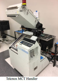 Tekmos sells many micro controllers and Flash memories that are in PLCC packages. These mature packages are not being supported by modern handlers, and so we are fortunate to have acquired both a number of MCT handlers, and production kits for packages sizes ranging from 20-pin PLCC up to 84-pin PLCC packages.
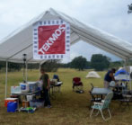 Tekmos Team Members returned to Oxford Ranch in the beautiful Texas Hill Country the first weekend of November. Lynn and Phil arrived first to set up the Tekmos pavilion with a help from You Tube as it was the first time for the two of them to set it up. Mission accomplished. Jon, Kelsey, Allan and Tyler arrived later and set up their tents and sat around the fire visiting until turning in. During the night rustling of a band of wild boars were heard nearby digging in the dirt for food. No one seemed too alarmed, not even furry companions.
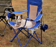 The following morning Jon, Kelsey, Allan and Tyler made their way to Enchanted Rock for a hike on the trails and a crawl through the caves. Enchanted Rock is such a popular destination that it closes its gates several times a day due to overcrowding. It is a massive 425' pink granite dome with 11 miles of hiking. Humans have been camping there for over 12,000 years and more than 400 archaeological sights have been discovered there.
 Other Tekmos Team Members, contractors and family members arrived in the afternoon for a few vigorous games of badminton and steaks grilled over a fire that evening.
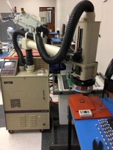 The temperature forcing probe is a washing machine sized box with an adjustable arm extending from it. At the end of the arm is a small test chamber. The machine can generate a temperature controlled stream of air, with temperatures ranging from -65ºC up to 185ºC. The test chamber is placed over the part, and the air is used to either heat or cool the part. Then we can measure the parts performance at a given temperature. And it has an auxiliary thermocouple that can be placed on the part to precisely control the actual part temperature.
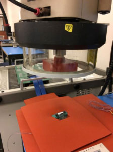 We do this for several reasons. When a new part comes out, we characterize its performance over the intended temperature range. Not only does this confirm the correct operation of the part, it also provides feedback for our design models. We also use the probe when we need to test production parts at temperature and do not have a temperature handler capable of working with a specific package. And finally, we use the probe for failure analysis when a customer reports a problem at a specific temperature.
 How long have you been at Tekmos and what brought you here?

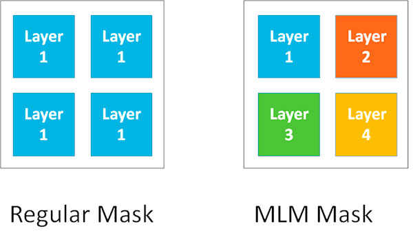
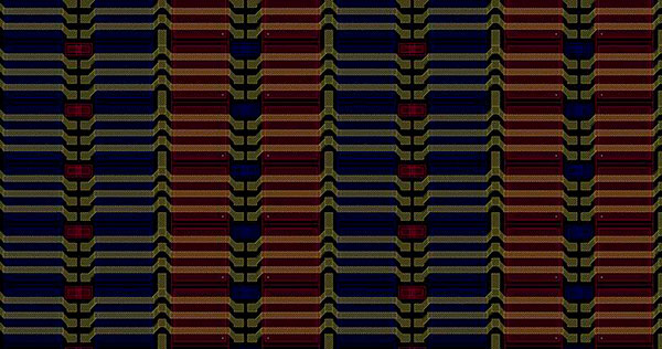
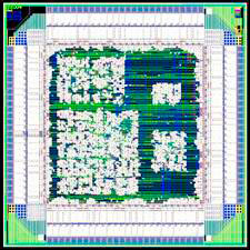
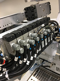 Tekmos make replacements for mature microprocessors. With the acquisition of Atmel, and we are seeing an increased demand for processors in the 40 pin DIP package. Whereas in the past, we have been dealing with small 100 piece orders, we are now faced with orders of up to 40,000. We had been manually testing the parts, but with the new, larger orders, we needed an automatic handler for testing.
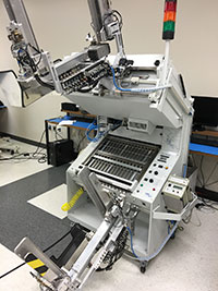 In this case, we found a high volume, tri-temperature, 600-mil DIP handler. There are a number of 600 mil DIP packages, including the 40-pin package. We bid on the auction, and won. The handler was in Germany, and so we had to have it shipped back to America.


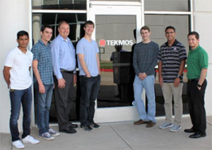
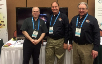
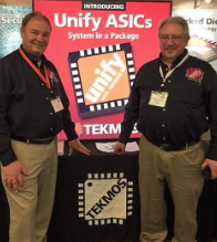
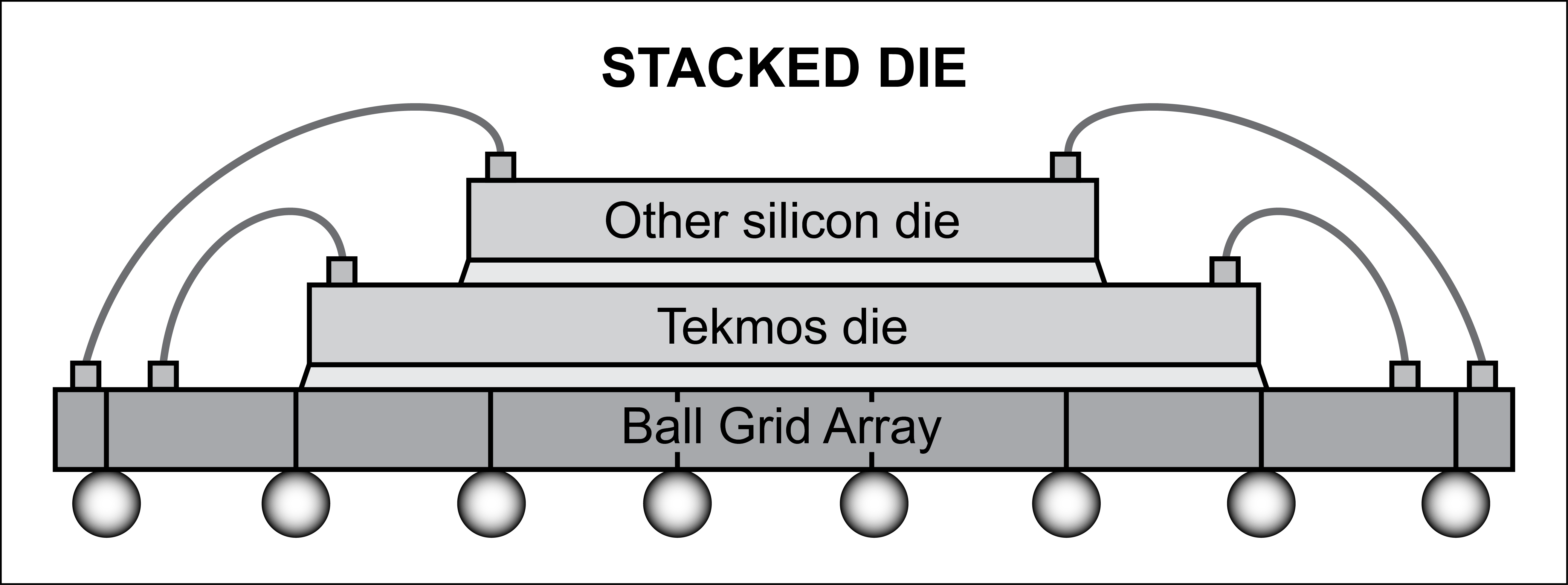
 When we travel on business, we try to take a little time to do something that is related to the place we are visiting. Not having much free time on this trip, our outing was limited to a stroll and dinner in