Tekmos Talks Newsletters
A newsletter for the semiconductor industry
Tekmos Talks 2014
|
|
||||
| A Newsletter for the Semiconductor Industry | ||||
| December 2014 | ||||
|
|
||||
| From the Desk of the President | ||||
|
Reviewing 2014 New Year's Resolutions Now that it is December, it is time to review my New Year's resolutions for 2014. I made 10 of them, and here they are. We will bring out programmers for our user programmable versions of our 68XX 80C51, and 28F010 families. Done. We have introduced the programmer for the 68HC711D3. While the other programmers are in progress, this has turned out to be a difficult task. We will develop new high temperature standard products. Done. We have three high temperature products in design. These are an 8051 processor, a 1553 bus driver, and an EEPROM with refresh and error detection and correction logic. We will also work on improving NVM performance at 175ºC. Done. We have shown that a refresh cycle is a valid method of improving memory retention at high temperature. The results of this work were published at the Hi-Tec Conference last May. We will bring out 0.18 micron ASICs. We missed this one. The growth in the high temperature area consumed the resources that we would have gone into 0.18u. We will expand our Japanese sales. Done. Our Japanese sales were up, and we continue to push forward in this area. We will expand our use of adapters as an alternative for obsolete packages. Done. We have sold three products this year on adapter cards. One was an ASIC that needed an adapter to replace a 256-pin PQFP package. One was our 68020 microprocessor that used an adapter to emulate a 132-pin BQFP package, and one was an adapter for our 80C186EC processor to emulate the 100-pin BQFP package. We will add a wafer probe capability. In progress. We have the probe machines, and are working to bring them on line. We will expand our high temperature (+175ºC) test capability. Done. We were using a temperature forcing probe to test parts. This required about 5 minutes per part, and was a serious capacity limitation. Now we have test boards that allow us to test about 50 parts per hour, and we can easily increase that amount as needed. We will complete the product qualification studies on our new 0.35u technology. Almost done. We have completed all tests except life test, and that is under way. We will perform multiple high temperature reliability studies at 175ºC. Done. We have collected a good deal of data at 175ºC, 190ºC and 210ºC. One thing that we have learned is that while the parts behave well, the test hardware deteriorates rapidly, and frequently fails beyond 2500 hours. Overall, I think that we have done pretty well. And definitely better than the resolutions I made for myself. |
||||
| New Product Announcement | ||||
|
New Product Launch, Flash Memories 28F010 Tekmos now offers the TK28F010, a 1024K (128K x 8) Flash Memory, to help solve obsolescence issues. It is a drop-in replacement for other 28F010 that many manufacturers are having trouble locating, due to discontinuance by other suppliers. This nonvolatile, random access Flash Memory is pin for pin compatible with other 28F010 memory. It has the same low current characteristics as other 28F010 memories and retains memory when the power is off. Having a drop-in replacement for parts has shown to be a very cost effective way to extend the life of products when the original component manufacturer discontinues a part. The availability of a drop-in replacement greatly simplifies the decision whether to redesign a printed circuit board or discontinue a product. The 28F010 memory is currently available in 32 plastic lead PLCCs. The 32 pin plastic DIP and the 32 lead TSOP versions can also be made available. Tekmos continues to be the "go to" supplier when there are problems finding obsolete parts or when additional parts are needed after the date for EOL (End of Life) purchase has passed. Tekmos makes a variety of microcontrollers, microprocessors, and other miscellaneous standard products to satisfy these needs. Tekmos also continues to make custom ASIC replacement parts. Customers are aware that buying from Tekmos ensures pin for pin, drop-in replacements that can be counted on to work in their applications, without worry about the quality of parts purchased on the grey market. |
||||
| Tekmos Travels | ||||
|
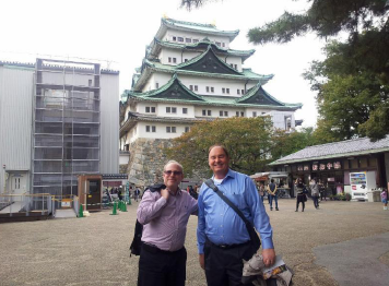
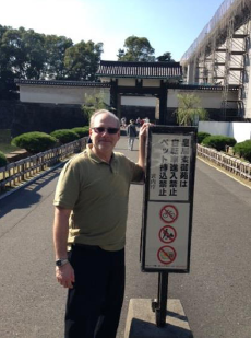
Travels to Japan Bob Abrams and I spent a week in Japan last month. The purpose of the trip was two-fold. First, we had scheduled visits with current customer to review project status. We also visited multiple prospective customers as part of our overall Japanese development strategy. From a business point of view, the trip was quite successful. We can summarize a business trip as being a plane trip, a hotel, a customer visit, back to the hotel, and then back to the plane. And after a while, all business trips can seem the same. I had decided a while ago to try to incorporate a little tourism into each trip, and this trip was no exception. After all, Japan is an interesting country, and it would be a shame to see nothing more than the inside of a hotel. On this trip, Bob and I were able to do two tourist things. Being old, I like to see things that are older than I am. So on a side trip to Nagoya, we visited the castle. Originally built in 1612, it has been restored, and is an interesting look into Japan's past. While having a military aspect, is was more of a palace for the Tokugawa family. The castle is topped off by two golden dolphins (Kinshachi), which is a tradition dating back to 1334. Bob and I also had a tea ceremony before we returned to Tokyo. Bob isn't as old as I, and wanted to see more modern things. So on the last day of our visit, we spent the afternoon looking at ham radio electronics, and then at other consumer electronics in Electronic Town (Akihabara) in Tokyo. I think we were both impressed with the modern toilets on display.
This was the first trip to Japan that I felt totally comfortable in using the subways. I always had a fear that I would become trapped below ground, going in an infinite loop because I could not read the signs for my exit. This time I had an app that told me when and where to change trains. And I learned where to read the station numbers. Once I had that down, we were free to go anywhere. After that, it was time to come back home. |
||||
| Meet Tekmos | ||||
|
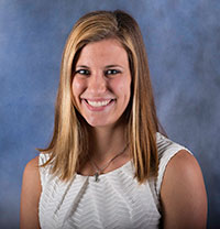
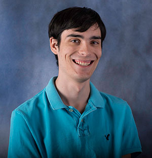
Kelsey Mehlhorn, Engineer Intern
I have been at Tekmos since October 22, 2014. I became interested in working here due to a recommendation from my aunt, Ruth Forkel, who is a consultant for Tekmos. What are your responsibilities here at Tekmos? I am responsible for component specifications and designing printed circuit boards (PCBs). What are your favorite tasks or projects to work on here at Tekmos? Since I've only been at Tekmos for a short time, my favorite task so far is designing these PCBs. What Project are you working on now? I am currently working on a PLCC 32 Pin MCT printed circuit board. Please tell us about your professional and educational background. I'm from The Woodlands, TX and am currently a 3rd year student at Texas State University, San Marcos. I am majoring in Manufacturing Engineering with a concentration in Mechanical Systems and a minor in Applied Mathematics. My current GPA is 3.6. I was an employee for Bath and Body Works premium outlets for almost two years; I became a seasonal manager the last year I was there. Prior to being hired at Tekmos, I worked at Petsmart a few months. In my spare time, I enjoy scuba diving, working out at the gym, and spending time with friends & family. |
||||
|
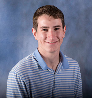
Will Grote, Test Operator
I started working at Tekmos in July, I was referred by a previous employee who I shared a class at Austin Community College Pinnacle with. What are your responsibilities here at Tekmos? My responsibility lies on the test floor, I am part of the production phase of Tekmos. I test parts and keep machines running and ensure the product gets out the door. What are your favorite tasks or projects to work on here at Tekmos? My favorite tasks are preparing goods to be shipped, and something we call "Shake & Bake", which is the process of transferring parts from test tubes to rails so that we can bake every milligram of moisture out of each part. What Project are you working on now? Currently hot testing which essentially does the same function under more extreme conditions, provided the test site is 175º C. Please tell us about your professional and educational background. I graduated from Austin High school in 2013, I am currently attending Austin Community College and looking forward to transferring to a four year college. I am an Eagle Scout as well as many of my coworkers. |
||||
| Thank You for Reading Tekmos Talks | ||||
|
Thank you for reading Tekmos Talks and helping us celebrate 20 plus years. Sincerely, Lynn Reed, President
|
||||
|
|
||||
| A Newsletter for the Semiconductor Industry | ||||
| November 2014 | ||||
|
|
||||
|
Welcome to Tekmos Talks October. We will be discussing "Our New Testers", introduce a new product, talk about company events, and share about the Tekmos website updates. |
||||
| From the Desk of Director of Operations, Jon Ghem | ||||
|
Quality Control & ISO 9001 Tekmos works hard to provide first-rate customer satisfaction and has completed all required audits and passed re-certification of its ISO 9001. Tekmos is resolute to provide the best service and highest quality in the industry. With state-of-the art equipment, experienced industry experts and cost productive solutions, Tekmos is dedicated to fulfilling the quality needs of our customers. In that quest for excellence we have enhanced our methods of getting feedback from customers by creating a "Tekmos customer survey" found on our website and provided here for your convenience. We invite you to take the short survey and tell us what you think about our products, customer service, website, or anything else you would like. Tekmos further encourages each customer to conduct an on-site quality audit of our processes and facilities to ensure they receive the quality they deserve when purchasing from us. For more information about Quality Assurance, please contact Jon Gehm, Director of Operations. |
||||
| New Product Announcement | ||||
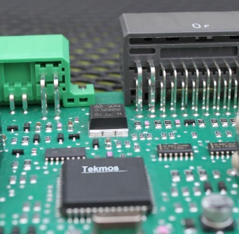
Packaging The guts of most durable products today contain a lot of electronics. The external package, whether an iPhone, a TV, or even a washing machine, is usually just the outermost package of multiple layers of packaging. In this article, we will look at innermost package type, the packaging that protects the IC (Integrated Circuit, sometimes called a computer chip.) Today, silicon chips are made with a very large number of transistors arranged to make digital logic. The transistors are very small, allowing hundreds of thousands, sometimes millions, of transistors, to be made on a thumbnail-sized piece of silicon. A major problem is how to connect signal lines and how to protect the IC from damage. Special electronic packages have been developed to accomplish these tasks. Advances in chip processing techniques have allowed for larger chips with smaller transistors. As this trend toward higher levels of integration (the inclusion of more circuitry onto a piece of silicon) continues, the number of signal lines has also increased. The package size has grown to accommodate the larger number of signal lines. The demand for the packages with low pin-count has declined significantly. As the volume falls, the economy of scale goes away. The volume decrease causes the unit cost to increase, putting additional downward pressure on its usage. Then another factor comes into play. The tools to produce any given package type are expensive. A plastic package requires not only a mold and a small piece of metal called a lead frame, it also requires tooling for finishing. As these expensive tools wear out, a choice must be made whether to replace them. The manufacturer must decide if possible future revenue justifies the expenditure for the replacement tooling. Often, it is not practical to continue making some package types. What do you do if you have a product that has a PCB (Printed Circuit Board) designed for a certain package type? If your PCB has a footprint that exactly matches the placement of connections on a particular package type, how do you proceed if nobody makes a package that fits that footprint? One costly approach is to design a new printed circuit board with a footprint for a similar device in a package that is available. The cost to design the new PCB, debug and test it, and update the documentation can be prohibitive. If the PCB was designed a long time ago, the designers may have moved on leaving incomplete documentation. Often manufacturing does not have a budget for design work. Solutions are even more costly when a new design requires a lot of testing such as for FDA approval.
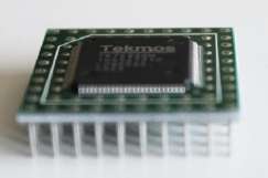
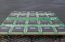
Another proven approach is to use an adapter card that interfaces between the needed footprint on the PCB and the circuit function in an available package. The adapter card cost is often much lower than the PCB redesign cost. Perhaps more importantly, the adapter card becomes a project for the chip maker rather than for the PCB assembler. Often, Tekmos can design a new silicon chip that performs same circuit function but placed in an available package. Tekmos can also have the adapter card designed and built so that the new packaged IC will mount on it. The adapter card will fit the original footprint. From the contract manufacturer's perspective, there is now a drop-in replacement for the unavailable part. |
||||
| Inside Tekmos | ||||
|
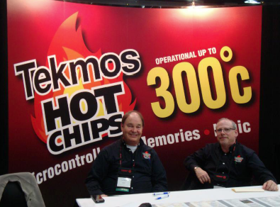
Last month Tekmos traveled to exhibit at another high temperature conference. This time it was the GEA Geothermal Energy Expo 2014 at the Oregon Convention Center in Portland, Oregon. The expo is billed as "the world's largest gathering of vendors providing support for geothermal resource exploration, characterization, development, production and management." Since the folks from Tekmos have spent most of their careers involved with microelectronics, it was fascinating to talk with the attendees and vendors who manufacture and use the massive equipment associated with the geothermal industry. Even though the exploration for and harnessing of geothermal energy makes use of equipment that is thousands of times bigger than our microelectronic circuitry, many pieces of equipment cannot function without the much smaller electronic components like those that Tekmos designs and manufactures.
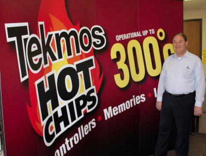
The expo gave us a chance to talk in depth with various equipment vendors about the performance and electrical characteristics they need most when choosing components for their new products. We were again reminded of the need to listen carefully and to clarify terms. Some of the vendors at the Expo talked about their requirement for maximum operating temperatures of 300 degrees without mentioning they were speaking in degrees Fahrenheit. Others at the conference needed 250 degrees operating temperature, without mentioning they were speaking in degrees Celsius, the units generally used in the electronics industry. The 300 degrees Fahrenheit, about 150 degrees Celsius, is pretty straight forward for Tekmos using standard bulk silicon technology but 250 degrees Celsius will require our SOI processing. This second high temperature conference of the year for Tekmos yielded a number of new contacts as well as a chance to visit with other customers that we have known for some time. We also received a number of inquiries about our standard products where the high temperatures are not required. There were even some inquiries about Tekmos supplying parts that are going obsolete by the original vendors. While this has been a major focus of Tekmos throughout its 17 year history, we were a little surprised since our focus at this geothermal conference was "Hot Chips", our relatively recent thrust into the high temperature market.
As we often do, we also took some time to visit a local attraction. We had a tasty lunch at a great Chinese restaurant suggested to us by a local who thought we looked lost as we got off the light rail. We were primed for our visit to Portland's Lan Su Chinese Garden, the most authentic Suzhou-style Chinese garden outside China. Its name is poetically interpreted as "Garden of Awakening Orchids." It was assembled by 65 Chinese artisans who spent 10 months assembling and completing structures that were crafted in China. From the Hall of Brocade Clouds, past the Scholars Courtyard, to the Tower of Cosmic Reflections, the Garden is a sea of tranquility near center of the bustling city of Portland. It was a welcome period of peace and quiet between our travel to Portland and our manning the booth at the Geothermal Expo. |
||||
| Meet Tekmos | ||||
|
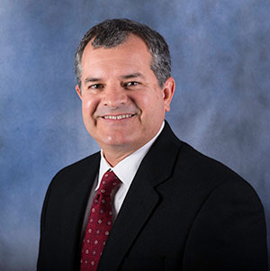
Alan Reed, I.T. Administrator
How long have you been at Tekmos and what brought you here? I have been working on and off for the past 6 years, and full time for the past 6 months. What are your responsibilities here at Tekmos? I am responsible for the programmer we send to customers, IT problems, and implementing an electronic workflow system. What are your favorite tasks or projects to work on here at Tekmos? My favorite task has been to work on the programmer we send to customers. I have always enjoyed creating something from scratch and continually adding to it. What Project are you working on now? I am currently working on implementing an electronic workflow system using the program Alfresco. Please tell us about your professional and educational background. I graduated from Westlake High school and attended the University of North Texas where I studied Computer Science. During my breaks I would work for Tekmos, and that turned into a full time job. |
||||
| Thank You for Reading Tekmos Talks | ||||
|
Thank you for reading Tekmos Talks and helping us celebrate 20 plus years. Sincerely, Lynn Reed, President
|
||||
|
|
||||
| A Newsletter for the Semiconductor Industry | ||||
| October 2014 | ||||
|
Welcome to Tekmos Talks October. We will be discussing "Our New Testers", introduce a new product, talk about company events, and share about the Tekmos website updates. |
||||
| From the Desk of the President, Lynn Reed | ||||
|
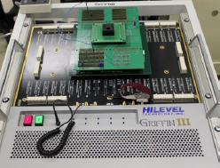
Our New Tester Every part that Tekmos manufacturers, has to be tested. The wafer manufacturing process will naturally produce a percentage of non-functional parts, and we must identify them and reject them. Tekmos uses a combination of inside and outside test resources to test the parts. Tekmos has experienced sizable growth over the last two years, and as a result, we were finding ourselves limited by our test capacity. To address this, we decided to buy additional testers to augment the two testers we already had. Purchasing a tester is a complicated decision. You need to determine how many pins the tester will need. Most of our devices have less than 100 pins, though some have 356 pins. Since tester cost is generally a linear function of pin count, it is important to buy the right amount of pin capacity. You must also consider the economic tradeoffs of tester speed and vector memory capacity. After months of internal deliberations, we decided to purchase a new Griffin III tester from HiLevel. This tester has 128 pins with a 64M vector depth and a 100 MHz clock rate. This is a significant increase in our capability, since our older testers were limited to 40 MHz and 8M of vector depth.
While we were negotiating over the Griffin III tester, we found another HiLevel on the surplus market. This one was a model ETS780 tester, with 256 pins and an 8M vector depth. It is a much older tester, but was a valuable at a reasonable price, so we acquired it as well. Along with the testers, we have acquired a new problem. Each tester has a different mechanical interface. In the past, we have just built a custom interface for a specific part to connect to a specific tester. However, this approach has caused capacity problems as our volume has increased. We frequently find ourselves in a situation where we need two different parts that are only testable on a single tester. This results in the situation where one tester is running two shifts, while an adjacent tester is standing unused. Our solution to this is to create an interface that will connect any tester to any hardware. Since many of our products are tested on a handler at the end of a cable, we are going to make that cable interface standard. One part of that standard is to assign the tester channel number to always be connected to part pin number. Channel 1 to connect to pin 1, and so forth. Normal industry practice is to assign tester channels to pins in a pattern that produces equal physical lengths. This allows the maximum timing accuracy. In our case, we do not need that level of accuracy. Most or our designs are old, and do not have critical timing specifications. It does not matter if signal A arrives 500 picoseconds before signal B. Converting to the new system will be a slow process. We have perhaps 30 different boards to re-do. So we will start with the new products, and gradually extend the process to the higher volume parts. We may never convert some of our very old parts. But for the important parts, we will have flexibility. Parts from 1 to 64 pins will run everywhere. Parts from 65 to 128 pins will run on 3 testers. Parts from 129 to 256 pins will run on two testers, and parts from 257 to 320 pins will still only be supported by one tester. Now that our tester capacity problems are addressed, we will turn our attention to our next test problem, which is adding a probe capability to our test floor. |
||||
| New Product Launch | ||||
|
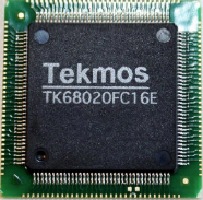
Tekmos has added an additional microprocessor to further grow its line of chips: the TK68020. The TK68020 is a full 32-bit implementation of one of the members of the 68000 family of microprocessors from Motorola. The TK68020 is functionally equivalent to earlier versions of the 68020. It is both pin-for-pin compatible and object-code compatible with earlier members of the 68000 family. The TK68020 also has some added additional features. The TK68020 is currently available in an adapter that fits the 132 pin BQFP footprint. |
||||
| Tekmos Travels to Geothermal Energy Expo 2014 | ||||
|
Tekmos executives traveled to the Geothermal Energy Expo in Portland, Oregon September 28 thru October 1, 2014. The Geothermal Energy Expo, in its 38thyear, is the world's largest gathering of vendors providing support for geothermal resource exploration, characterization, development, production and management. Tekmos enjoyed the opportunity to showcase its high temperature state of the art "Hot chip" technology to the geothermal community and a brand new Trade Show Display.
|
||||
| Tekmos Website New Look | ||||
|
Tekmos has been enjoying an incredible growth of its product line and in keeping up with that growth the Tekmos website has also expanded. We thought that this would be a good opportunity to share the updates, new additions and sections to Tekmos' website. We want to provide all visitors to the Tekmos site ease so we improved the "contact us" template to give visitors an opportunity to request specific needs. A "Management" section highlighting the Tekmos' Executive Team has been added under "Corporate Info". Tekmos' goal is service and quality, and our benchmark for quality is from the customer's view. In that light, Tekmos "Support" section has been expanded with a "Quality Corner" created to share news to customers about our quality control protocol. In addition, and in accordance with the U.S. Dodd-Frank Act, a "Conflict Minerals Reporting" was added. The "What's New" section has also seen some changes with more additions of Press Releases and a section about "High Temperature Faqs" as Tekmos "Hot" Chips" increases interest in the oil and gas, military, medical, and geothermal energy industries. "Inside Tekmos" offers website visitors an opportunity to learn more about Tekmos Team members and company events.
|
||||
| Thank You for Reading Tekmos Talks | ||||
|
Thank you for reading Tekmos Talks and helping us celebrate 20 plus years. Sincerely, Lynn Reed, President
|
||||
|
|
||
| A Newsletter for the Semiconductor Industry | ||
| September 2014 | ||
|
Welcome to Tekmos Talks September. We will be discussing "Reliability Studies", introduce two new products, and talk about upcoming events. |
||
| From the Desk of the President, Lynn Reed | ||
|
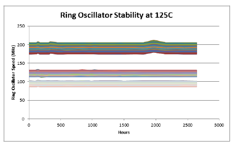
Long Term Reliability Studies Tekmos makes a wide variety of parts, and as a result, it can be complicated to compare reliability results over different parts. To address this, we incorporate a common reliability monitor into most of the parts we make. This monitor is designed to detect small changes over time due to the most common reliability problems. Specifically we are looking for threshold shifts due to either hot electron injection or DC bias. We detect the shift by measuring the frequency of an embedded ring oscillator. If a threshold shift occurs, the ring oscillator will change frequency, and that can be detected and measured. We connect a number of individually addressable microcontrollers on a board. We then communicate with the board while it is in the oven, and have each processor measure the frequency of the various ring oscillators in the reliability monitor. The results are reported and stored on an external computer. This article will talk about two studies we are doing on our 0.6u process.
This is a plot showing the individual frequency measurements made on 3 sets of ring oscillators, in 77 devices, over 2500 hours and at 125ºC. The key thing to note is that after this time, there have been no long-term changes in the measurements. There are times when all ring oscillators are running faster. This is because we share our ovens between reliability experiments and production dehydration bakes. Occasionally, our measurements coincide with the loading of the ovens with production material. When that happens, the oven temperature temporarily drops, and the lower temperature causes the ring oscillators to run faster. The upper band of readings comes from a ring oscillator that is made from inverters. It is constantly running, and is looking for threshold shifts due to hot-electron injection. The middle and lower bands represent ring oscillators made of NAND and NOR gates, respectively. These ring oscillators are normally off, and are only turned on for measurement. Being off, they have a DC bias on their gates most of the time, and are used to look for threshold changes over time due to bias. This would measure the presence of contaminates in the oxide.
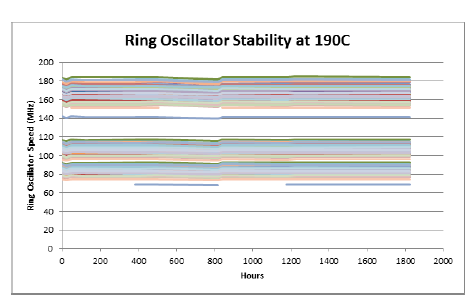
This plot shows the same information as the above plot, except that the oven temperature is 190ºC. We are doing the high temperature testing for down-hole applications in the oil industry that requires these temperatures. As a side benefit, the oil studies provide excellent qualification data for parts operating at lower temperatures. All of the above reliability data are based on our 0.6u process. We use this process in our 68XX microcontrollers and in many military circuits. We also collect similar data for our 0.35u and our 1.0u SOI processes. While many reliability experiments run for only 1000 hours, we plan to continue collecting data this type of data for at least a year (8000 hours), and perhaps longer, depending on the availability of oven space. |
||
| New Product Launch | ||
|
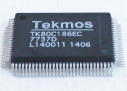
Tekmos has expanded its line of microprocessors with two 80C186 microprocessors: the TK80C186EC and the TK80C188EC. The Tekmos 80C186 series has been carefully designed to duplicate the original 80C186 in all aspects except for co-processor support. The TK80C186EC and TK80C188EC will work correctly at either 3 or 5 volts. The original Intel parts were sorted by minimum operating voltage to select parts for the "L" series. With today's improved process control, it is possible for all Tekmos parts to operate at both 3 and 5 volts. Orders for the "L" series will be filled with "C" parts. The TK80C186EC is available in 100 pin PQFP. They are direct, pin for pin, replacements for the S80C186EC. The availability of the TK80C186EC and the TK80C188EC are additions to the already available TK80C186EB and TK80C188EB. These additions to the TK80C186 line of microprocessors join the 80C51, 78HC05 and 68HC11 microprocessors already in production at Tekmos. |
||
| Tekmos Travels to Geothermal Energy Expo 2014 | ||
|
Tekmos executives will attend the Geothermal Energy Expo in Portland, Oregon September 28 thru October 1, 2014. The Geothermal Energy Expo, in its 38thyear, is the world's largest gathering of vendors providing support for geothermal resource exploration, characterization, development, production and management. Tekmos is looking forward to the opportunity to showcase its high temperature state of the art "Hot chip" technology to the geothermal community. Geothermal energy is thermal energy generated and stored in the Earth. Thermal energy is the energy that determines the temperature of matter. The geothermal energy of the Earth's crust originates from the original formation of the planet (20%) and from radioactive decay of minerals (80%). The geothermal gradient, which is the difference in temperature between the core of the planet and its surface, drives a continuous conduction of thermal energy in the form of heat from the core to the surface. The adjective geothermal originates from the Greek roots γη (ge), meaning earth, and θερμος (thermos), meaning hot. (Wikipedia) Iceland is a pioneer to the rest of the world in the use of geothermal energy for space heating largely due to the high concentration of volcanoes. Geothermal power facilities currently generate 25% of the country's total electricity production. |
||
| Thank You for Reading Tekmos Talks | ||
|
Thank you for reading Tekmos Talks and helping us celebrate 20 plus years. Sincerely, Lynn Reed, President
|
||
|
|
||
| A Newsletter for the Semiconductor Industry | ||
| August 2014 | ||
|
|
||
| From the Desk of Director of Operations, Jon Gehm | ||
|
A chain is a fascinating thing. Look up the definition. I have seen it explained as "a series of things depending on each other, as if linked together." Most people at first thought will visualize iron rings, physically linked through each other, stretching from one point to another. The linkage is strong, dependable and permanent. But is this idea true? What of the saying that a chain is only as strong as its weakest link. Hidden in that vision of strength, a weakness may exist, unknown until challenged. At a crucial time this vision of strength may break, resulting in the destruction of the linkage. It is interesting that the single weakness is able to produce a failure of the entire interdependent system. The result is a system unable to provide strength, and a system that is no longer dependable. All of this failure is traced back to a single weakness within the chain. A chain may come in many different forms. There is the chain of command, allowing teams to work together under a hierarchy of leadership roles. There is also a chain of events, where one occurrence leads to another, then another, until a final, perhaps even unforeseen outcome results from the series of interdependent events. Then there is what we consider to be the most important chain of all. At least it is to Tekmos, and to our customers. This is the production chain. The series of companies that work together, each dependent on the other, to provide the product our customers' trust us to deliver. Recently, I took the opportunity to visit links in our production chain. I visited i2a Technologies and Pantronix Corporation, each in California. The visit was not to audit, or inspect. The visit was to say hello, and how can we work better together. While I always learn something when I visit another company, from the way the teams organize themselves, to the quality standards, and all of the other intrinsic processes that build these organizations. There is one important constant I try and never forget. The constant is that companies are made up of people. And the better that people from different companies get along and work together, the stronger the relationship becomes. In this day of emails, and texts and with the avalanche of electronic gadgetry, the simple cup of coffee, with the off the cuff conversation of current events and where do you find the best steak, is easy to overlook and lose. To have a strong chain, you need strong relationships with people. At Tekmos we understand the theory of the chain. We understand its strength and its potential weakness. We work to build our production chain, not just with processes, but with one hello and one friendly visit at a time. A strong supply chain creates a trusted product. And a trusted product is what our customers demand, and what they deserve. |
||
| Get The Lead Out | ||
|
Getting the Lead Out
The ancient Romans not only used lead pipes for water, they preferred it for vessels to hold wine, saying it made for a sweeter taste than copper vessels. There has been a lot of speculation, with scientific basis, to show that lead poisoning, especially of the elite, may have been a major contributor to the fall of the Roman Empire. Lead was causing us problems over two thousand years ago! Lead has been shown to be such a major contributor to health problems that lead is banned from paints currently used in most countries. The problem of young children getting lead poisoning from eating old paint chips in dilapidated inner city homes is still a problem today. Retardation in toddlers has been traced to the acid in orange juice leaching lead from the glaze on drinking cups. Why are we using lead in the first place? Simply said, it has very desirable features, if one can ignore the fact that it is killing us. The Romans found the lead to be easy to work with for pipes and containers. Lead can help make paint more elastic so that it does not crack as easily with some expansion and contraction with temperature. It also can contribute to a nice glaze on ceramic cookware, if you do not mind poisoning your family or blowing out your microwave due to its conductive properties. The EU directive, Restriction on Hazardous Substances, RoHS, came into effect on July 1, 2006, prohibiting the inclusion of significant quantities of lead in most consumer electronics produced in the EU. This has become the de facto standard that we follow. While the elimination of lead affects many industries, the effect on the electronics industry is especially large. The major questions are: what do we use in place of lead and what new problems will be introduced? In electronics, lead, especially when combined with tin, makes a great "glue" to hold wires together and components onto printed circuit boards. In combination with tin, the melting point of the compound can be lower than for either lead or tin separately (the eutectic point). Not only is it a good conductive glue, its melting point is nearly ideal. At about 185C (355F), it does not melt until well above commercial, industrial and military operating temperatures. And it melts at a temperature much below the point where plastic packaging melts or other damage is done to sensitive components. Tin, combined with other metals such as silver and copper, show much promise for lead free solder, but there are many metallurgical issues such as tin whiskers and joints becoming brittle. Each combination has a higher melting point than the lead-tin alloy. With the same maximum processing temperatures for the components, this is a significant narrowing of the window of acceptable processing temperatures. These, and many related problems are being solved, but there is much more work to be done. The next time you hear "Get the Lead Out" remember this has been a problem for humanity for over two thousand years and we are still working on the problem. |
||
| Tekmos Welcomes KW Electronic Sales | ||
|
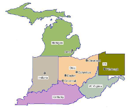
Tekmos is pleased to announce KW Electronic Sales as a manufacturing representative. KW Electronics has successfully represented quality electronic component manufacturers since 1969 starting in Dayton, Ohio, expanding in 1974 to Pennsylvania, into Kentucky followed with Indiana and Michigan in 2000. President, William Hardman says, "Everyone in the company is an electrical engineer and we have plenty of experience working with semiconductor companies. We look forward to growing Tekmos Line." KW Electronic Sales serves a diverse range of customers who require a variety of components in varied markets, from military, transportation, medical and industrial requiring a need for long term product support. Tekmos helps customers continue to support long term programs containing discontinued products yet still satisfying current applications and additionally keeping their costs down. Hardman says, "As an example, power plants and specifically nuclear power plants whose control systems are strictly regulated operate 30 or more years requiring long term product support. We offer that guaranteed support." KW Electronic Sales territory covers the 6 state area of Western Pennsylvania, West Virginia, Kentucky, Ohio, Indiana and Michigan. William Hardman, President will pass the reigns over to Deborah Henderson next year but plans to stay on in an advisory capacity and continue to represent specific accounts. For more information KW Sales: William Hardman at 412-559-9985 whardman@kwsales.com or Deborah Henderson 513-659-9811 dhenderson@kwsales.com
|
||
| Thank You for Reading Tekmos Talks | ||
|
Thank you for reading Tekmos Talks and helping us celebrate 20 plus years. Sincerely, Lynn Reed, President
|
||
|
|
| A Newsletter for the Semiconductor Industry |
| July 2014 |
|
Welcome to Tekmos Talks July. We will be discussing "Obsolete Device Package Types", introduce |
| Featured Product |
|
The TK80C186EC The TK80C186EC microprocessor, the Tekmos version of the 80C186EC, is now in production by Tekmos. The TK80C186EC is available in 100 pin PQFP package and, using an adapter card, the 100 pin BQFP. The 80C186 was originally an Intel design. Since its inception, a number of companies have made different versions of the 80C186. Tekmos developed an 80C186 core design that can be used to replace many variations of the 80C186. The Tekmos 80C186 design was carefully designed to duplicate the original 80C186 in all aspects except for co-processor support. One variation of the 80C186 is the 80C186EB. Tekmos offers this as the TK80C186EB / TK80C188EB which directly replaces the Intel 80C186EB / 80C188EB microprocessors. They are available from Tekmos in the 80 pin SQFP package and the 84 pin PLCC 84. The 80 pin PQFP package is available on request. The TK80C186EC is a direct replacement for the Intel 80C186EC, another variation of original 80C186. Tekmos added a DMA controller, an interrupt controller, and more parallel ports in developing this current version. It is available in a 100 pin PQFP and adapted 100 pin BQFP. While the actual 100 pin BQFP package is not available, Tekmos has made an adapter card version which directly fits the 100 pin BQFP footprint and outline. Look for the Tekmos article on how Tekmos adapter cards circumvent the problem of obsolete packages. See the article below. |
| Obsolete Devices |
|
Obsolete Devices & Package Types- A Solution Ever need a part in a package that is no longer available? Many older products have designs with components in obsolete packages. Not only are packages like BQFPs almost impossible to find, more commonly used packages, such high pin count DIPs, PLCCs and PQFPs, are becoming rare or non-existent. It is expected the newer QNF style packages will make the availability of older package types go away even faster. Even if the silicon chip inside could be obtained, there may be no manufacturer willing to make the needed package anymore. Even it were possible to get someone to begin making the package again, it would be so expensive that it could not be used. It is just not in the interest of a packaging house to tool up for an obsolete package type. So, are you stuck with the choice of re-engineering the printed circuit board or discontinuing the manufacture of a product that continues to sell? Most companies do not have the resources to allocate to redesigning older products. The expense of engineering for new part type is high. Even just redesigning a new Printed Circuit Board layout for a new package footprint, debugging the new board, and introducing the change to the factory is often so high that discontinuing the product seems the only option. Tekmos has been providing a solution to this problem for many of its customers. The solution has two parts: redesigning a functionally equivalent silicon chip and finding a way to have a packaged silicon chip fit the same footprint as the original part. Tekmos will redesign the function of the obsolete part into a new, functionally equivalent silicon die. Sometimes this is done from the original specification for the part, although it is significantly easier when the design files and test vectors are available. Of course, this does not solve the package problem but it does give a working, usable silicon chip. The second part of the solution is the introduction of an adapter card. The Tekmos designed equivalent silicon chip is assembled in a package that is readily available in today's market. A small adapter card is designed that has the same footprint and lead configuration as the original part. The new chip, in the new package type, is mounted on the adapter card. The adapter card is mounted on the original Printed Circuit Board in the same manner that the obsolete part was mounted. The result has the needed function in the newly designed silicon chip with the same mounting characteristics as the original part. It is the introduction of the adapter card and the readily available alternative package type that makes the whole assembly usable in place of the obsolete part. Tekmos has provided a variety of parts with adapter cards to fit the existing Printed Circuit Boards. If the problem of obsolete parts, even in an obsolete package, is a problem you face, contact us to see if we can help you. |
| Hi Temperature FAQs |
|
Tekmos is pleased to announce its new High Temperature FAQs page. The following are the first few FAQs: Q1) What is the maximum temperature for Tekmos High Temperature ICs? Tekmos has two types of high temperature offerings: Bulk Silicon and SOI. The first is pushing bulk silicon substrate devices to the temperatures where leakage becomes excessive, a little over 200ºC. The second, newer SOI processing is expected to yield devices that will work to a little over 300ºC. Q2) What is the history of Tekmos in the high temperature market? Tekmos has been developing libraries and related technologies for high temperature applications since 2010. Our 175ºC TK68HC811E2 began production in 2014. Our first 250ºC ASIC was shipped in 2012. There are currently five high temperature products in design at Tekmos: EEPROMs, FPGAs, ASICs, the TK80H51 and the TK68HC811E2. We presented papers at the International Conference on High Temperature Electronics in 2013 and 2014. Q3) How does SOI differ from older silicon technologies? SOI is an acronym for Silicon On Insulator. The more commonly used CMOS (Complementary Metal Oxide Semiconductor) technology inherently has a path for current leakage through the bulk semiconductor. Since SOI does not have this path, the leakage will be significantly less. This leakage results in excessive current. With the typical semiconductor, the leakage becomes so large around 200-225oC that the devices no longer work. While there are other leakage paths in SOI technology, they are usually not a problem until temperatures reach about 300oC or greater.
|
| Thank You for Reading Tekmos Talks |
|
Thank you for reading Tekmos Talks and helping us celebrate 20 plus years. Sincerely, Lynn Reed, President
|
|
|
||
| A Newsletter for the Semiconductor Industry | ||
| June 2014 | ||
|
|
||
| Featured Product | ||
|
The TK68020 Works! We received news that our first pass TK68020 was working in the customer system. A first pass success. This has been a huge project that has taken us over two years to complete. It started with extracting the design from the original layout as a spice netlist. The design was converted into spice primitives, and then into Verilog, and all of the components were converted from dynamic logic to static logic. It was then simulated, and modified to remove race conditions. Next, it went into layout. The data path structure of the chip required months of manual floor-planning. We also had to re-implement the microcode ROMs as true ROMs instead of logic. During this process, our original fab closed, and all work had to be transferred to a new fab. We also had to deal with the original BQFP132 package becoming obsolete. The package problem was resolved by using a 144 pin TQFP package and an adapter card. Recognition is due to Lynn Reed for the original circuit extraction, John Hoenig for the design conversion and simulation, and James Betts for the floor planning and other layout tasks. |
||
| Tekmos Hi Tec Conference 2014 | ||
Last month, Tekmos presented a paper at the HiTec conference. HiTec is dedicated to high temperature electronics, ranging from the relatively cool 175C up to the 1200C range for Silicon Carbide. It also covers high temperature materials and passive components. The Tekmos paper investigated the use of refresh cycles to assist with data retention in EEPROMS. We are developing a new 256K, high temperature, and high reliability EEPROM. At elevated temperatures, the charge stored in the memory leaks away, and must be replenished. While an EEPROM at 85C can be expected to hold the data for 10 years, at higher temperatures (~200C), the data retention time is measured in days. Restoring the data is made more complicated since the number of times that an Erase-Write cycle can be used also decreases with temperature. The 100,000 cycles guaranteed at lower temperatures becomes 100s of cycles at high temperature. We get around this by using a refresh cycle. A refresh cycle does not do an erase prior to the write, and so can only be used to re-write the same data. We were concerned that repeated refresh cycles could also cause damage, but our experiments showed that a refresh cycle is safe. To prove this, we set up a system using our TK68HC11E1 devices, which contain 512 bytes of EEPROM. This is the same basic EEPROM cell that we will use in our 256K EEPROM. We attached 77 of the microcontrollers to a board, and configured them so that we could communicate with a specific microcontroller. Then we downloaded programs into the microcontrollers, and ran experiments. The experiments included such things as determining the number of Erase-Write cycles it took to burn out an oxide, or just giving the part a fixed number of refresh cycles. This made it easy to collect a large amount of high quality data that was the basis of our paper. For the first time, Tekmos had an exhibit at HiTec. We showed our TK68HC811E2 high temperature microcontroller, and our 250ºC ASICs. We also provided a preview of our 256K EEPROM, our 250ºC TK80H51 microcontroller, and the TKH4003 FPGA. These last three products are under development, and we will be introducing them over the next year. One advantage of exhibiting at a conference is that it provides feedback about what customers really want to see in products. It also shows what the competition is doing. Together, that provides invaluable marketing guidance for our own efforts. The conference is small, with about 300 attendees. Still, this was one of the best shows that we have ever exhibited at. The crowd was highly focused, and almost every booth conversation was of high quality. We have been to shows that were 30 times larger, and gone away with a fraction of the leads we got from HiTec. We will definitely be exhibiting at the HiTen conference next year in England. |
||
| Inside Tekmos | ||
|
Business trips are usually intense. You work hard, and are frequently up late in the evening. To compensate for this, we try to add a little extra to each trip. This month, four of us went to the HiTec conference in Albuquerque. We had free time for dinners, and 5 hours at the end of the conference between the show closing at noon, and having to be at the airport at 5. That was plenty of additional time for something extra. Albuquerque has a 10K foot mountain in the city limits, called Sandia Peak. There is a restaurant located on top of it, which you access by a tram. We decided to have our Wednesday dinner on top of the mountain. It was a beautiful 20 minute tram ride up there. Once there, we were unable to eat due to lack of reservations, so we went to the bar, and ate off of the bar menu. I also had a conference call while up there, which I took while standing on a rock ledge, overlooking Albuquerque 5,000 feet below. It was cold up there, and there was still snow on the ground. But the views were incredible, and well worth the cold. We stayed up there until dusk, and then took the tram back to the car. After the conference ended we went to see the Petroglyph National Monument. This monument contains a number of Indian petroglyphs dating from 1300 AD that are carved into blocks of lava on the west side of Albuquerque. We walked along several of the trails checking out the petroglyphs. There were hundreds of them to view. Being an amateur geologist, I was also impressed by the lava flow. We were in a small canyon that at one time had been a hill. The lava had flowed on either side of the hill. In a mere 200,000 years, the hill had eroded, leaving the the canyon we were in. After checking that out, we toured the National Museum of Nuclear Science & History. This is much better suited for engineering nerds, with its collection of rockets, old airplanes, bomb casings, and old radios. I particularly enjoyed studying the engines of a Titan II rocket. I had seen a detailed description of the SpaceX rocket engine, and so I knew what I was looking at. It was also interesting to study the avionics and wiring harnesses used in the planes and rockets. We have done a number of these "extra" events, but this was definitely one of the best. The Indian Pueblo Cultural Center offers 1 hour guided tours of the museum. If you want to visit some of the Pueblos near Albuquerque please find the interactive map and note pueblos are on tribal land. |
||
| Thank You for Reading Tekmos Talks | ||
|
Thank you for reading Tekmos Talks and helping us celebrate 20 plus years. Sincerely, Lynn Reed, President
|
||
|
|
| A Newsletter for the Semiconductor Industry |
| May 2014 |
|
|
| Featured Product |
|
TK68HC811E2
The TK68HC811E2 is one of our older processors, and dates from the late 70s. It uses the HC11 core, and is noteworthy in that it has 2K bytes of EEPROM. In an era when all other micros were One-Time-Programmable (OTP), it was one of the first re-programmable processors. As such, it found its way into many industrial systems and is still in use today. This was an evolutionary dead end for Motorola. The EEPROM could not keep up with the densities being achieved with EPROM, and so Motorola did not use the EEPROM approach with other members of the HC11 family. Nonetheless, the part has survived to the present time. When Tekmos started to reverse engineer the HC11 family, we created a common gate array to implement the different family members on. We chose to include 768 bytes of EEPROM on this array, along with 768 bytes of RAM, and 24K of ROM. We did so for extreme environments knowing that this prevented us from making the 68HC811E2, as well as the 68HC11F1, which had 1K of RAM. Then we came across an opportunity for the 68HC811E2. The opportunity was large enough for us to create a new gate array for the chip. We are exhibiting this month at the HiTec conference in Albuquerque, and will be featuring this part there. |
| Tekmos in Albuquerque May 13-15, 2014 |
|
Stop by & Visit Tekmos, Inc. at the: International Conference on High Temperature Electronics (HiTEC 2014) Albuquerque Marriott Pyramid North Albuquerque, NM May 13-15, 2014Tekmos will showcase the hottest innovations in high temperature technologies with our "chip" experts onsite to assist with your design challenges. Join us for our technical session presentation Wednesday, May 14 : The Effects of Repeated Refresh Cycles on the Oxide Integrity of EEPROM Memories at High Temperature Presented by Lynn Reed and Vema Reddy. Session WA1: Si Chair: Randy Normann, Perma Works LLC 8:00 am - 11:30 am HiTEC 2014 continues the tradition of providing the leading biennial conference dedicated to the advancement and dissemination of knowledge of the high temperature electronics industry. Under the organizational sponsorship of the International Microelectronics Assembly and Packaging Society (IMAPS), HiTEC 2014 will be the forum for presenting leading high temperature electronics research results and application requirements. It will also be an opportunity to network with colleagues from around the world working to advance high temperature electronics. Papers will be presented in the following areas:
|
| Things to do in Albuquerque |
|
Albuquerque, New Mexico is known as the "Hot Air Ballooning Capital of the World", for its surrounding pueblos, and its deep cultural history. The Anderson Abruzzo International Balloon Museum provides visitors with a history of ballooning. The Indian Pueblo Cultural Center offers 1 hour guided tours of the museum. If you want to visit some of the Pueblos near Albuquerque please find the interactive map and note proper etiquette when visiting as pueblos are on tribal land. Tekmos engineers and executives plan to learn more about the Atomic Age by visiting the National Museum of Nuclear Science & History located at 601 Eubank Blvd. S.E. in Albuquerque. It is the nation's only congressionally chartered museum in its field and a Smithsonian affiliate. For the adventurous and T.V. fan, there is The Breaking Bad RV Tours offering 3½ hour tour travels to 17 of the show's most popular locations. Tours are offered daily. |
| Thank You for Reading Tekmos Talks |
|
Thank you for reading Tekmos Talks and helping us celebrate 20 plus years. Sincerely, Lynn Reed, President
|
|
|
||
| A Newsletter for the Semiconductor Industry | ||
| April 2014 | ||
|
Welcome to Tekmos Talks April. This month we will share about "Bringing up a New Fab", "High Temperature Testing", and upcoming news and product development for Tekmos. |
||
| From the Desk of the President | ||
|
Bringing Up A New Fab Over the past nine months, Tekmos has been qualifying a new fab for our 0.35u production. There are a lot of steps involved with that that I will review here. Fortunately, there are a lot of similarities in the available 0.35u process. A well designed part that works in one process will likely work the same way when manufactured in another fabs 0.35u process. The challenge is in the conversion from one process to another. The conversion starts with the layout rules. The rules from both fabs must be compared and differences identified. In our case, the rules had one major difference: the gate length for 5 volt transistors increased from 0.5u to 0.6u. An increase in length of 500 atoms may not seem like a lot, but it caused a lot of problems. In a gate array architecture, the key design parameter is the routing grid that is used for interconnect. There are many variables that influence the grid, but one of the main ones is the center to center spacing of two contacts with a gate between them. When this changed, the entire routing grid changed, and that meant that we could not reuse our existing layouts. Instead, we had to create a new technology based on the new process. As with all new technologies, we study the layout rules, and create DRC checks to verify that our new layouts are compliant with those rules. We check our work by creating a structure that contains each layout rule with a good and bad case. Then we run our DRC checks on that structure to validate the checks themselves. Next we create the "block" that contains the transistors that we use to build everything else. A block typically consists of three pairs of transistors. Why three? This is a tradeoff between efficiency in building a logic gate, and the waste if a given gate doesn't use all of the resources. As with most things in life, the optimum is "e", or 2.71. Since we must use whole transistors, we have a choice between 2 and 3 pairs. We chose 3 pairs. Most companies use 3 pairs. Some use 2 pairs, and a few use 4 pairs. Once we have a block, we build up our library of logic gates. For the most part, our library is unchanged between the different technologies that we use, and this time was no exception. Using a common library prevents mistakes in creating new technologies, and makes it easier for designers to use the libraries. The new library is subjected to LVS and DRC checks before it is added to the place and route library. We also use the block to build up gate arrays. In our new 0.35u process, we have created gate arrays with 127K gates (176 pads) and 270K gates (256 pads). We will create at least two more, smaller gate array sizes in this technology. Once the block has been designed, we know the transistor sizes, and so we then run spice runs to collect the data that we use in creating the Synopsys libraries. That is used to create the SDF files necessary to properly simulate the designs. Then we start making chips. But we are not done. We take a few of the first chips and measure the ESD and latch-up (LU). We also put parts into a 1000 hour HTOL test at 125C, and determine if there is any fallout. We embedded our reliability monitor into one of the first parts, and that will give us detailed results for hot electron failures, threshold shift under bias, and metal migration. We also evaluate the first parts, and confirm their actual performance matches the performance predicted by the spice runs. And that is how we bring up and qualify a new process. |
||
| High Temperature Testing | ||
|
High Temperature Testing
The basic handlers go to 150ºC. And while it would be possible to boost the temperature to 175ºC by modifying the controller in the handler, that could cause many other problems, such as damaging part of the handler, or even starting a fire. One could create an extender cable, and put a socket in an oven. That works, but there is a cycle time associated with ovens, and the throughput would be measured in parts per hour. We would also like to minimize the time that a test operator has to work in front of an open oven door. Our approach is to create a board with multiple sockets on it. This shares the cycle time over many parts, and so our throughput goes up into the 100 part / hour range. Having multiple parts on a board introduces test problems. A part has 48 wires associated with it. 50 parts has 2400 wires. This is a huge bundle, and the logistics of dealing with it are overwhelming. So we have to develop a better solution. All of our parts are microcontrollers. As such, they can communicate serially. If we give each controller a different address, then we can connect all microcontrollers with a total of 6 wires: 2 supplies, reset, clock, transmit and receive. With the wire problem solved we now have one last problem: how to actually test the processors. Each processor has a bootstrap mode that allows a program to be downloaded externally. We can use this program to exercise, and thus test, each portion of the processor. It takes a while, but since the processors can be running in parallel, the overall throughput is not affected. And that is how we hot test parts. |
||
| Tekmos News & Product Development | ||
|
|
||
| Thank You for Reading Tekmos Talks | ||
|
Thank you for reading Tekmos Talks and helping us celebrate 20 plus years. Sincerely, Lynn Reed, President
|
||
|
|
||
| A Newsletter for the Semiconductor Industry | ||
| March 2014 | ||
|
Welcome to Tekmos Talks March. This month we will share news about our TK80C186EC processors, SOI parts, and introduce a Tekmos team member. |
||
| From the Desk of the President | ||
|
TK80C186EC Processors We shipped our first TK80C186EC processors in February. There was a lot of effort behind that statement. We started with our 80C186EB processor, and added the DMA channels, and changed the interrupt controller to the 8259A style. There were a few other changes, such as adding power-down modes in the clock generator. Plus, we had to make the design work on a process from a different fab. And that entailed the creation of physical and simulation libraries. There was a lot of work and now we have the first part. The next step is to transfer the part from engineering into production. There is a combination of product engineering, test engineering, and marketing efforts. The product engineering task is to characterize the part, and verify that the measured performance lies with the design limits, and exceeds the original data sheet limits. Since we use newer processes on all of our replacement parts, it is never an issue to exceed the original data sheet. But it is good to know that actual distribution of our parts, since we set the test limits based on that distribution. This way, we can fail a part that falls outside of the normal distribution, even though it may meet the original part specifications. The next step is to release the test program. Our test programs typically consist of an Iddq test, followed by two passes of the functional patterns. One pass is at a high voltage, and the other is at the lowest specified voltage. These passes also check input levels and AC specifications. Then we have special passes to measure the output current levels and input high impedance. Once the test engineer is happy with the test, it is released for production. The marketing of the part means that we will create a web page for it, post the data sheet, and enter it into the Google ad-words program. And we will write an article about this for our newsletter. Which is what this is, and so now we are done. |
||
| SOI | ||
|
SOI Process Revision
Tekmos made our first SOI parts two years ago. When we set up the first gate array, we made some decisions that in hindsight were not good. More specifically, we established a routing grid that increased density (good), but at the cost of potential DRC errors from the autorouter (bad). We had done this previously with our 0.35u process, and it resulted in 3 or 4 DRC errors per chip. These were easily corrected by hand, and was not a problem. In our first SOI ASIC, we had thousands of DRC errors, and it took weeks to correct. This was a real problem, in that it was always possible that we might find ourselves with a future chip that had so many errors that it might not be possible to correct all of them. We chose to use a slightly larger routing grid which allows the router to work without any DRC errors being created. We had a second problem in that we set the gate width too small. As a first order approximation, the gate width does not matter. Since gates drive gates, doubling the width doubles the load, and so the speed remains the same. But there is another component to load and that is the interconnect capacitance. If the capacitive load is too great, then we have to insert buffers in the wire to maintain speed. Increasing the transistor width reduces the need for these buffers, and simplifies the place and route task. These actions work but it also requires us to re-layout hundreds of cells in our cell library. But once that is done, we now have a strong library that will allow us to exploit the 250C market with high temperature microcontrollers, FPGAs, and memories. |
||
| Thank You for Reading Tekmos Talks | ||
|
Thank you for reading Tekmos Talks and helping us celebrate 20 plus years. Sincerely, Lynn Reed, President
|
||
|
|
||
| A Newsletter for the Semiconductor Industry | ||
| February 2014 | ||
|
Welcome to Tekmos Talks February. The new year is promising to keep us busy with our customers and ongoing innovation. This month's newsletter will talk about Flash Memory Emulation, introduce another Tekmos Executive, and an update on TK68020. |
||
| From the Desk of the President | ||
|
Flash Memory Emulation In addition to ASICs and microcontrollers, memories also become obsolete. One of our projects is a replacement for an obsolete Intel 28F010 flash memory. This is a 1 MB, 5 volt, flash memory, and does not have any sectors. Unlike our other products which use standard processes, flash memories use a dedicated process. And once that memory has become obsolete, the wafer fab is usually converted over to a newer process so that it can make newer flash memories. This causes customer problems since the newer flash memories use lower voltages, and frequently have different programming algorithms. As a result, the customer is faced with a system redesign because the older parts are not available. We can't recreate the old process. What we can do is to use one of our ASICs as an interface between the old application and a newer flash memory. We then buy flash die, and assemble both the flash memory and our ASIC in a single package that now works in the old application. This approach has several interesting engineering issues. First, we have to design a voltage regulator so that the external 5 volt supply is stepped down to the 3.3 volts required by the memory. And it Lynn Reed, President has to have a fast response to changes in load current, because when a flash switches to write mode, the current can increase from 10ua to 50 mA in a few microseconds. Another problem is the write algorithm. Flash memories have a write algorithm that is used to prevent accidental writes to the memory. For this chip, we have to detect when the write algorithm occurs, and replace it with the write algorithm required by our chip. And since there is no clock available, we have to turn on a ring oscillator and make our own clock. A third problem involves the use of high voltages. The Intel part uses ~13 volts to indicate the programming and to enable a special device mode to read the manufacturer's ID. Our part will self-destruct if a voltage greater than 7 volts is applied to it. To get around this, we have to put an internal resistor between the VPP pin and our internal detect circuit that will limit the voltage that the part actually sees. A fourth problem occurs when using our device in some programmers. They will immediately remove the power from our part after the write is finished. Unfortunately, we require a little time to finish our own write algorithm, and so we will fail in some programmers. I don't think that we will be able to solve that problem, and so we will have to provide our own programmers, or we will have to ask the various programmer companies to alter their algorithms for us. And that is how we make Flash memory replacements. |
||
| Meet Tekmos | ||
|
|
||
| Tekmos TK68020 | ||
|
TK68020 Update It has been a while since I have talked about our 68020 development so it is time for an update. The basic design flow in this project was to extract a transistor level netlist from the layout, convert it into standard, synthesizable logic, verify it in an FPGA, and then make it. We are now in layout, though like everything else in this project, layout has also been a difficult task. Creating a hierarchical transistor level netlist from the layout started out tough, until we developed some procedures that greatly simplified the task. Next we developed software that identified the basic gates and replaced the corresponding transistors. The complex logic gates were next, followed by the dynamic flops and latches. However, the design didn't simulate in Verilog. So we used whole chip Spice simulations to debug the Verilog. This pointed to issues in our interpretation of the clock drivers, and then the chip began to work. Eventually, we had the chip passing all 51 Freescale test vectors. But, and this is a big but, the netlist contained a lot of dynamic logic. So our next step was to convert all of the dynamic logic into static logic. This was a difficult task. In particular, the data buses were frequently used as dynamic latches, and proved to be difficult to convert into normal logic. We also had a lot of problems with dynamic multiplexors, which was a type of latch with 3 to 4 inputs and the same number of enables. Eventually, these were resolved, and the netlist was released to layout. And this is where the next set of problems occurred. The design has a lot of 32 bit busses; at least 10 that I can think of. The buses are driven by a small tri-state driver that occupies one block, and has 4 signals going to it. This is a high density of signals, and can cause routing problems. This is aggravated by the tendency of the autorouter to place all of the tri-state drivers next to each other, producing an unroutable ball of logic. So we have been doing a manual placement of the data path. There are a lot of cells, and so we have been placing the data path for a month now. When that finishes, we will auto-place and route the rest of the circuit, tape out, and have prototypes 8 weeks later. It has been a long project (2 years), and we are looking forward to the end. |
||
| Thank You for Reading Tekmos Talks | ||
|
Thank you for reading Tekmos Talks and helping us celebrate 20 plus years. Sincerely, Lynn Reed, President
|
||
|
|
||
| A Newsletter for the Semiconductor Industry | ||
| January 2014 | ||
|
Welcome to 2014 & Tekmos Talks first newsletter of the year. This month's newsletter will share New Year's Resolutions, introduce a member of Tekmos' executive team, and talk about low cost reliability studies. Happy New Year! 2014 is going to be another "hot" year! |
||
| From the Desk of the President | ||
|
2014 New Year's Resolutions Another year has passed, and it is time for the company New Year's resolutions. Some of them look suspiciously like last year's resolutions. Product Development and Sales
Manufacturing
Quality
|
||
| Meet Tekmos | ||
|
|
||
| Tekmos Reliability Studies | ||
|
Low Cost Reliability Studies Ongoing reliability studies can be expensive. The burn-in boards are populated with expensive sockets, and can cost around $10K each. These burn-in boards can also require expensive driver boards, adding another $10K to $20K to the setup charges. And the burn-in boards have a limited life, and may need to be replaced every year or so. There are lower cost methods for burn-in. We usually burn-in microcontrollers, and realized that we can take advantage of the intelligence in the micro to reduce costs. With only six wires, (VDD, Ground, RX, TX, reset, and clock), we can talk to the micros while they are in the oven being burned in. We can wire up each micro with a different address, and that allows us to communicate with each one individually. Once we establish communications, we can download various test programs, and perform a complete test on each part while it is in the oven. Most of our micros have a built in reliability monitor that checks for threshold drift and hot electron injection. This can also be accessed during burn-in. And that provides a large amount of data on a continuous basis during the burn-in. Since we can test the part in the oven, we do not need to use sockets. Instead, we can just solder the parts onto the burn-in board. This reduces the burn-in board costs down to a few hundred dollars. When taken together, we have a very low cost system for continuous reliability studies. And that lets us afford to do even more studies. |
||
| Thank You for Reading Tekmos Talks | ||
|
Thank you for reading Tekmos Talks and helping us celebrate 20 plus years. Sincerely, Lynn Reed, President
|
||
Main Office
Tekmos, Inc.
14121 Highway 290 West
Building #15
Austin, TX 78737
Phone: (512) 342-9871

 Welcome to Tekmos Talks December and Happy Holidays. We will revisit Tekmos' 2014 New Year Resolutions, introduce a new product, talk about travels to Japan, and introduce two Tekmos Team Members in "Meet Tekmos".

 How long have you been at Tekmos and what brought you here?
 How long have you been at Tekmos and what brought your here?

 Welcome to Tekmos Talks August. We will be discussing "Getting the Lead Out", introduce a new rep for Tekmos, share about a vendor visit, and talk about "Inside Tekmos".
 Most people have heard the expression "Get the Lead Out" to refer to someone who is moving too slowly; implying that they can move faster if they get rid of weight that is slowing them down. A different and fascinating way to hear this expression is to take it literally, to see what it means, why this is important, and how long it has taken.
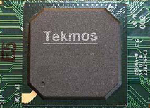 our new High Temp FAQ's page, and talk about a new product, the TK80C186EC
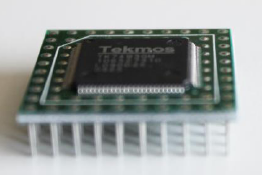
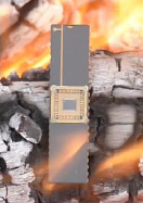
 Welcome to Tekmos Talks June. The Hi-Tec 2014 "International Conference on High Temperature Electronics" was a great success for Tekmos. This month's newsletter we will talk about the Hi-Tec Conference, share news "Inside Tekmos," and talk about a new product.
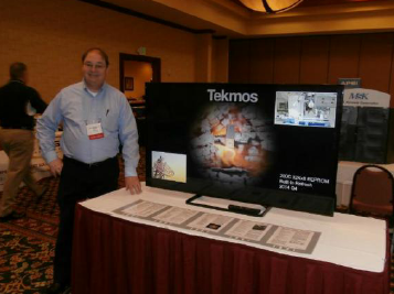
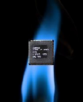 One issue in selling high temperature circuits is proving that they work at high temperature. And that means testing at high temperature. One of our products is rated at 175ºC.