-
This email address is being protected from spambots. You need JavaScript enabled to view it.
Tekmos' Blog
Tekmos' Blog
Stacked Die and IoT
Most silicon die are packaged in one of a wide variety of packages. The package protects the die, the wire bonds, as well as supplying an interface to the larger geometries of PCBs (Printed Circuit Boards). Since the beginning of the use of packaged silicon, most packages contained a single silicon die.
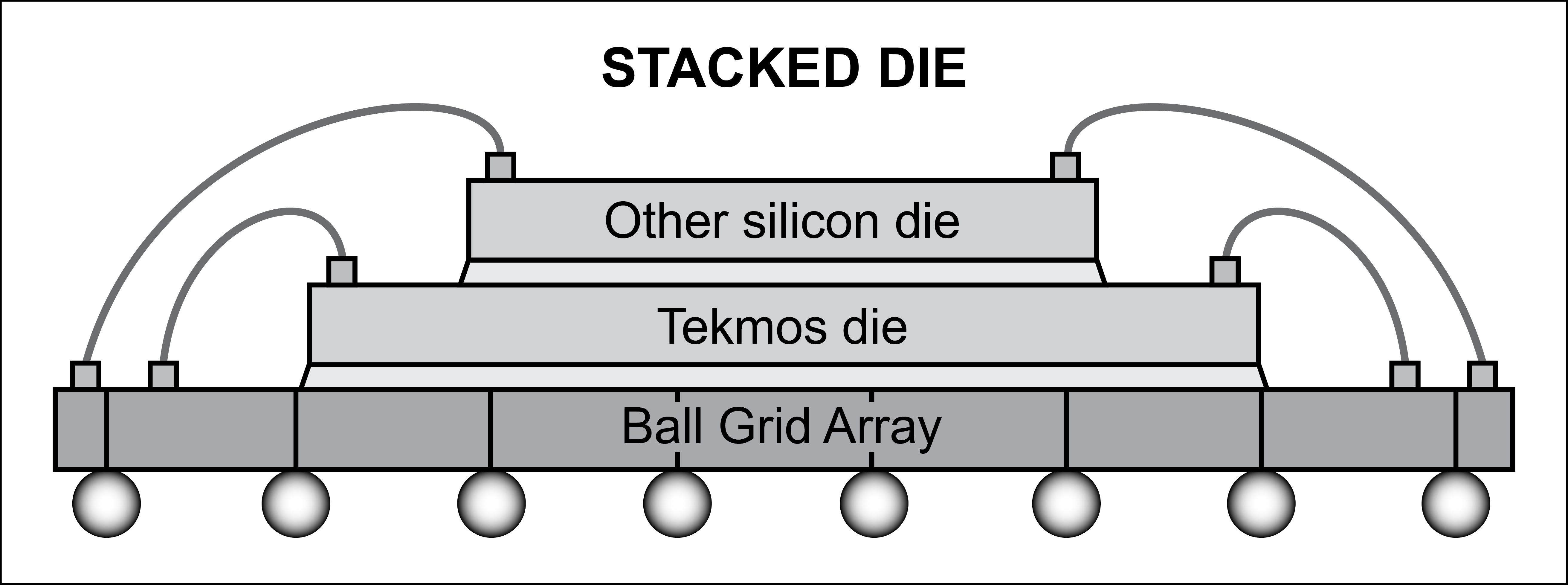
In the past few years, the assembly technique of mounting one die on top of another within the same package has become more widely accepted. Many of the problems of attachment of the die and rules for wire bonds have been worked out, even for high volume production. There is even talk of whether this Stacked Die approach will replace SOC (System On a Chip).
Cost is an obvious advantage of stacked die. First, there are fewer parts on the final assembly on a PCB. More importantly, different silicon processing techniques can be used for each silicon chip in the stack. Each part is optimized for its function and even the silicon processing can be optimized. Often, these parts of the overall design have found widespread use in many applications, driving the cost of the die by the economies of scale.
The use of stacked die also has a major positive effect on design activities. If a block of circuity already exists, there is no need to redesign it, saving significant engineering time and cost. Additionally, this lowers risk and increases the likelihood of first time success since, at least this part of the design, is known to be good.
One example is a design that requires a unique structured IC with a large amount of Flash memory. Since a Flash die can be purchased, there is no need to include it in the customized structured design. The process used to fabricate the structured design will not need to include the silicon processing steps required for Flash. The customized structured design will have a higher yield and lower cost since it has less circuitry. The higher yield and less expensive processing of the structured design also helps push cost down. Without redesigning the flash circuitry, the design time and cost are lowered.
Much of the IoT world requires features that almost describe the stacked die approach. The final overall design is made smaller with stacked die. Handheld electronic devices are one of the major reasons for the rapid advance of the stacked die approach. Then again, an IoT device for tracking the location of a cat or cow cannot be very large either. Time to market is reduced by lessening the amount of design time and increasing the probability of first time success.
A new idea for an IoT product can get market share quickly by the use of already made building block chips plus an underlying structured device. The breadth of electronic components that can be stacked is quite wide and the limit is primarily imagination. The use of Stacked Die is expected to be a major method of implementing designs in IoT applications.
When you subscribe to the blog, we will send you an e-mail when there are new updates on the site so you wouldn't miss them.