

Deprocessing a Die
As part of the netlist extraction process, we take an original die, and cut it apart one layer at a time. Each layer of the die is imaged with a scanning electron microscope. Then the image in converted into a GDS data base. Subsequent steps extract the netlist from the GDS database.
This article shows the deprocessing steps, and the resulting GDS database for a small section of a chip. This particular chip uses a double metal, double poly technology. The section shown is a digital section, and did not use poly2, so that step is skipped.
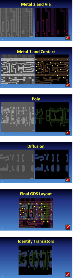 The first image shows the metal 2 layer. The vias show up well in this image, so we can extract both the metal 2 layer and the via layer. Conductive layers show up brighter in a SEM micrograph. But only the metal 2 layer shows up. The metal 1 layer in under the intermetallic layer, and so does not appear bright in this image. This is good, since if the metal 1 layer was visible, then it would be much harder to extract the metal 2 layer from the image.
The 2nd image shows the metal 1 layer. The contacts show up in this layer, but the vias do not. Some of the contacts show up as bright dots, and some show up as dark dots. Fortunately, the software is able to identify both types as contacts. There is a visible shadow on the image left over from etching away the metal two layer. This shadow is ignored by the software.
The 3rd image shows the poly1 layer. The diffusion layers also show up in this image. This is a difficult extraction, but can be made easier by looking at the diffusion layer apart from the poly1 layer. The imaging of the poly1 layer can be particularly difficult where it crosses diffusion in the creation of a transistor. There are spots that may have to be manually cleaned up.
Removing the poly1 layer makes the diffusion layers show up reasonably well. And speaking of wells, note that the p-well in this process does not show up at all. The presence of a p-well in the digital area can be easily inferred. It is tougher in cases where there may be a p-well resistor in the analog circuitry.
[Picture 4- “Diffusion”] This image shows the combined extracted database, which is a portion of a standard cell d-flop.
[Picture 5-GDS Layout”] This final picture shows how the software has identified the transistor locations in the layout.
[Final Picture “Identify Transistors”] The extraction of the GDS layout is relatively straight forward. Producing the hierarchical netlist from a listing of transistors is more difficult. I will discuss that process in a future article.
Date
2019-09-27

Wafers Edge Blog
Main Office
Tekmos, Inc.
14121 Highway 290 West
Building #15
Austin, TX 78737
Phone: (512) 342-9871