

Merged Designs
Implementing a design into an ASIC has many steps, some of which are expensive. One such item is the generation of the tooling or masks which are the physical embodiment of each layer. The masks are the tools. Each mask layer is costly to implement in a real physical sense since there is an enormous amount of detail with extremely small sizes and tight tolerances. When making larger quantities of one part type, the costs are amortized over a very large number of parts so that the cost per part is very low.
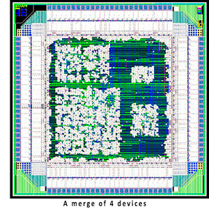
Are there any alternatives if there are only moderate volumes over which to amortize the mask charges? One approach that Tekmos has used successfully is to merge several design functions into one chip type. This can be an especially good approach if the number of required pads is large compared to the amount of circuity. In these cases the die size is dictated by the periphery with large amounts of unused area on the inner part of the layout.
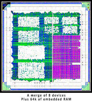
This allows the cost of the masks to be amortized over all the circuits. If the size of the die is not affected much, there will be very little effect on the per die cost. This approach has the added advantage of allowing a larger number of identical wafers to be processed further lowering the costs. Additionally, until the die are packaged, there is flexibility on the how the inventory of identical wafers are allocated.
The designs are merged into a single layout. The selection of which circuit is activated is done when the die are packaged. Different wire bonds are used to select which design is activated. This approach has allowed Tekmos to make several cost effective ASICs at moderate volumes.
The first picture shows the merging of four designs into a single layout. The second picture shows an actual physical layout that incorporates eight different designs plus some RAM. This is a very high number of devices merged but it illustrates what can be achieved.
Date
2015-10-17

Wafers Edge Blog
Main Office
Tekmos, Inc.
14121 Highway 290 West
Building #15
Austin, TX 78737
Phone: (512) 342-9871